What the Bluetooth PCB Tech Trends and Secret Applications ?
Abstract:
This post provides a thorough technical analysis of the Bluetooth PCB , a foundation of modern-day cordless connectivity. We will explore its technological advancement, from early concepts to the advanced standards of Bluetooth 5 and Bluetooth Low Energy (BLE). The text explores the vital design concepts, market characteristics, and transformative applications throughout different markets. For engineers, item developers, and technology lovers, this guide explains why comprehending the subtleties of Bluetooth PCB style and its ecosystem is important for innovating in the Web of Things (IoT) era.
Table of Contents
Intro .
The Bluetooth PCB (Printed Circuit Board) is the fundamental hardware that makes it possible for the common wireless communication we rely on everyday. For more years than Twenty, Bluetooth Innovation has quietly operated our earphones, speakers and external equipment. Nevertheless, its development has become quite sharp, pushed it beyond the basic point-to-point connection. Today, improvement markets such as Bluetooth low energy (BLE) and Aries networking are changing markets, making Bluetooth PCB clever buildings, advanced manufacturing, and wise city infrastructure to spread an important part in spreading.
This article acts as a definitive guide to the current state and future trajectory of Bluetooth PCB technology. We will dissect the crucial technological patterns, from the power-efficient design of BLE to the expansive capabilities of Bluetooth 5. Additionally, we will evaluate the useful applications and market forces driving this growth, offering important insights for anybody involved in electronic devices design, development, or tactical execution. We will likewise offer a technical look into the design factors to consider that engineers must resolve to produce a trustworthy and high-performing Bluetooth PCB .
What is a Bluetooth PCB and How Does it Function?
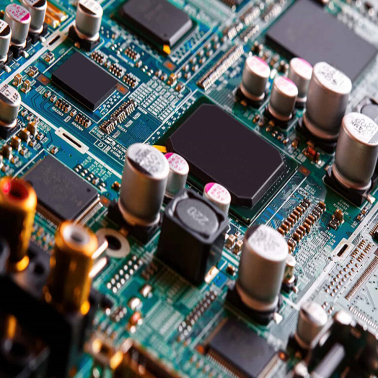
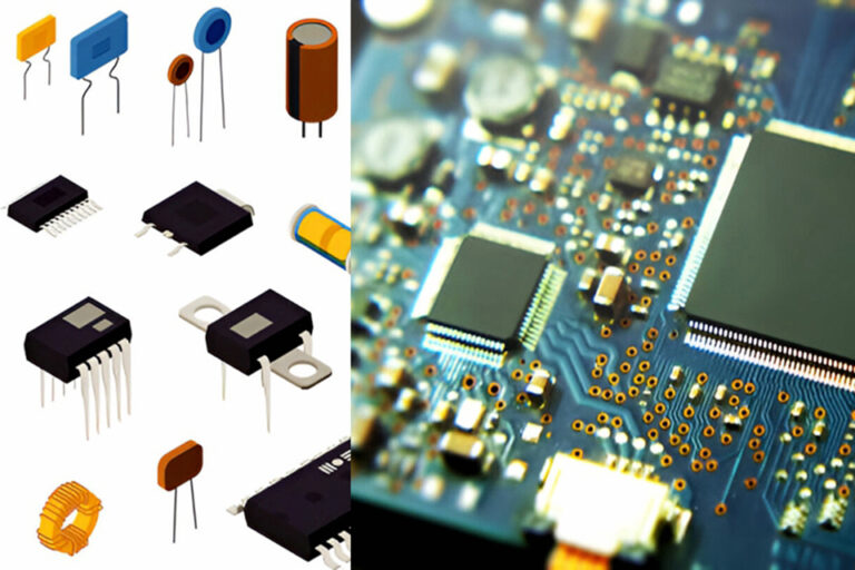
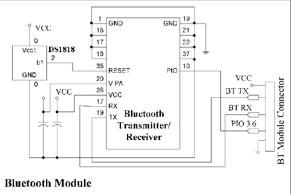
At its core, a Bluetooth PCB is a printed circuit board specifically crafted to host a Bluetooth communication chipset or module. This specialized board provides the essential physical and electrical infrastructure for the Bluetooth radio to run. Its function is to handle cordless data transmission and reception over the 2.4 GHz ISM (Industrial, Scientific, and Medical) radio frequency band. The board integrates a number of essential parts that work in unison to accomplish this.
The primary part is the System-on-Chip (SoC) or a pre-certified module which contains the Bluetooth radio transceiver and a microcontroller (MCU) . The MCU runs the Bluetooth protocol stack, which manages connections, security, and information packet handling. The PCB itself includes conductive paths, or traces , that route power and information signals in between the SoC, power management components, and the antenna. A critical part of any Bluetooth PCB is the antenna , which converts electrical signals into radio waves for transmission and vice versa for reception. The design of the antenna and its surrounding layout, referred to as RF design , is critical for attaining optimum range and signal stability.
Essentially, the Bluetooth PCB functions as the central nerve system for any Bluetooth-enabled device. It processes commands, manages power usage, and carries out the intricate job of sending out and getting information packages wirelessly. Whether it is a simple physical fitness tracker or an intricate commercial sensing unit network, the reliability and efficiency of the gadget hinge directly on the quality and design of its Bluetooth PCB .
How Did Bluetooth Evolve From a Basic Cable Replacement?
The journey of Bluetooth innovation began in 1994 at Ericsson, a Swedish telecoms business. Engineers developed it as a wireless alternative to the troublesome RS-232 data cables. The name “Bluetooth” admires Harald “Bluetooth” Gormsson, a 10th-century Danish king famed for uniting disparate Danish tribes, much as the innovation intended to unite various communication procedures. The initial requirements established a master-slave architecture. In this design, a single “master” gadget could link to and control up to 7 “servant” gadgets in a little network called a piconet.
This early architecture, referred to as Bluetooth Classic, was advanced for its time. It ran in the 2.4 GHz frequency band and utilized a strategy called frequency-hopping spread spectrum (FHSS) . This technique rapidly switches frequencies to alleviate disturbance and boost security, a feature that remains a trademark of the technology. Early applications focused on wireless headsets, keyboards, and mice, effectively removing wires however limited by fairly high power usage and a basic one-to-many topology. The servant devices in a piconet could not communicate straight with each other, creating a bottleneck at the master device.
The constraints of Bluetooth Classic became more apparent as the need for linked devices grew. The requirement for lower power intake, longer battery life, and more complicated network structures drove the development of brand-new requirements. The formation of the Bluetooth Special Interest Group (SIG) , a consortium of companies, developed a collective environment to steward the technology’s advancement. This collaborative effort led to breakthrough innovations like Bluetooth Low Energy and Mesh Networking, changing Bluetooth from an easy cable replacement into a foundational innovation for the Web of Things. The modern-day Bluetooth PCB is a direct result of this constant, market-driven evolution.
Why is Bluetooth Low Energy (BLE) a Game-Changer for PCB Design?
Introduction to Bluetooth Low Energy (BLE), also known as Bluetooth Smart, in 2010 variation with Bluetooth core requirements. 4.0 marked a decisive moment for cordless innovation. BLE was not just an old update; It was a basic redisine focused on applications of a new class. Its main design objective was to meet the lowest possible power consumption. This growth enables small, battery-powered gadgets to operate for years and even a single coin-cell battery. For Bluetooth PCB designers, it opened a new universe of possibilities. Ble achieves its remarkable energy performance through many creative mechanisms. Unlike Bluetooth classic, which preserves a continuous connection, Ble is operated in the “sleep” mode most of the time.
This ultra-low power profile straight influences Bluetooth PCB style. Designers can now utilize smaller batteries, resulting in more compact and lightweight final product. The lowered power requirements likewise simplify the power management IC (PMIC) circuitry on the board, possibly reducing both the expense of materials (BOM) and making complexity. BLE’s effectiveness is the core enabler for the massive expansion of IoT gadgets. Without it, the vision of a world with billions of interconnected, battery-operated sensing units would be economically and almost impractical.
What Makes Bluetooth Mesh Networking a Revolutionary Action?
This creates a powerful many-to-many interaction system. The advanced element of Bluetooth Mesh depends on its message-relaying capability. If one node wishes to send out a message to a node that runs out its direct radio variety, it can communicate the message through intermediate nodes. This “hopping” extends the reliable range of the network far beyond the ability of any single device. A message can propagate across an entire structure, factory floor, or urban area, developing a big, robust, and self-healing network. If one node stops working, messages can simply discover an alternative path through other readily available nodes, guaranteeing high dependability. This makes the Bluetooth PCB a foundation for large-scale control systems.
This technology is built on the structure of Bluetooth Low Energy, acquiring its low power intake. This allows for the development of large networks of battery-powered sensors and controllers. The implications are extensive. In wise buildings, a mesh network can link thousands of lights, heating and cooling vents, and security sensing units into a single, cohesive system for centralized control and energy optimization. In industrial settings, it allows asset tracking and condition monitoring throughout an enormous factory floor. The scalability and dependability of Bluetooth Mesh have elevated the humble Bluetooth PCB from a component for personal gadgets to an essential component of industrial and industrial infrastructure.
How Does Bluetooth 5 Enhance PCB Efficiency and Variety? .
Released in 2016, Bluetooth 5 represents a significant leap forward in the core capabilities of the innovation, straight impacting the design and capacity of every Bluetooth PCB . The Bluetooth SIG developed this version specifically to attend to the growing needs of the IoT. It presented three significant improvements over its predecessor (Bluetooth 4.2): doubled speed, quadrupled range, and eight times the broadcast message capacity.
This is vital for applications that need quicker firmware updates over-the-air (OTA) or require to transmit bigger information payloads, such as top quality audio or sensor logs. For a Bluetooth PCB , this means the associated MCU needs to be capable of processing data at this greater rate, but the core RF design concepts stay similar. The most remarkable enhancement is the prolonged variety. By using brand-new PHY (physical layer) alternatives, Bluetooth 5 can accomplish a theoretical line-of-sight variety of as much as 400 meters (or 200 meters in typical usage cases). This allows a single Bluetooth PCB to cover a whole home or little commercial building, lowering the requirement for network extenders.
Additionally, Bluetooth 5 increased advertising data capacity from 31 bytes to 251 bytes. This allows gadgets to relay very rich information without the need for connection. This is the technique behind advanced beacons that can send URL, depth product details, or location-specific information. Bluetooth 5 Similarly, other cordless innovations such as Wi-Fi include enhanced algorithms for co-existence, which share the 2.4 GHz band. This reduces disturbances and causes more stable and reliable connections, an important factor to consider in the RF design phase of Bluetooth PCB design.
Table 1: Contrast of Bluetooth Innovation Versions .
| Function | Bluetooth Classic (BR/EDR) | Bluetooth 4.x (BLE) | Bluetooth 5.x (BLE) |
|---|---|---|---|
| Primary Use Case | Audio Streaming, File Transfer | Low-Power Sensors, Beacons | IoT, High-Speed Data, Long Range |
| Max Speed | ~ 3 Mbps | 1 Mbps | 2 Mbps |
| Common Range | ~ 10 meters | ~ 50 meters | ~ 200 meters (line-of-sight) |
| Power Usage | High | Very Low | Very Low (equivalent to BLE 4. x) |
| Geography | Point-to-Point (Piconet) | Point-to-Point, One-to-Many | Point-to-Point, Broadcast, Mesh |
| Broadcast Capability | N/ | 31 Bytes | 251 Bytes |
| Secret Benefit | High Data Throughput | Extreme Power Effectiveness | Range, Speed, and Broadcast Capability |
What Are the Vital Style Factors To Consider for a High-Performance Bluetooth PCB?
Creating a Bluetooth PCB is not as simple as just putting a module on a board. It is a nuanced discipline of RF engineering where little information can have a significant influence on efficiency. The main goal is to guarantee optimal signal integrity and minimal interference, allowing the Bluetooth radio to operate at its full potential. A number of critical design considerations need to be carefully resolved.
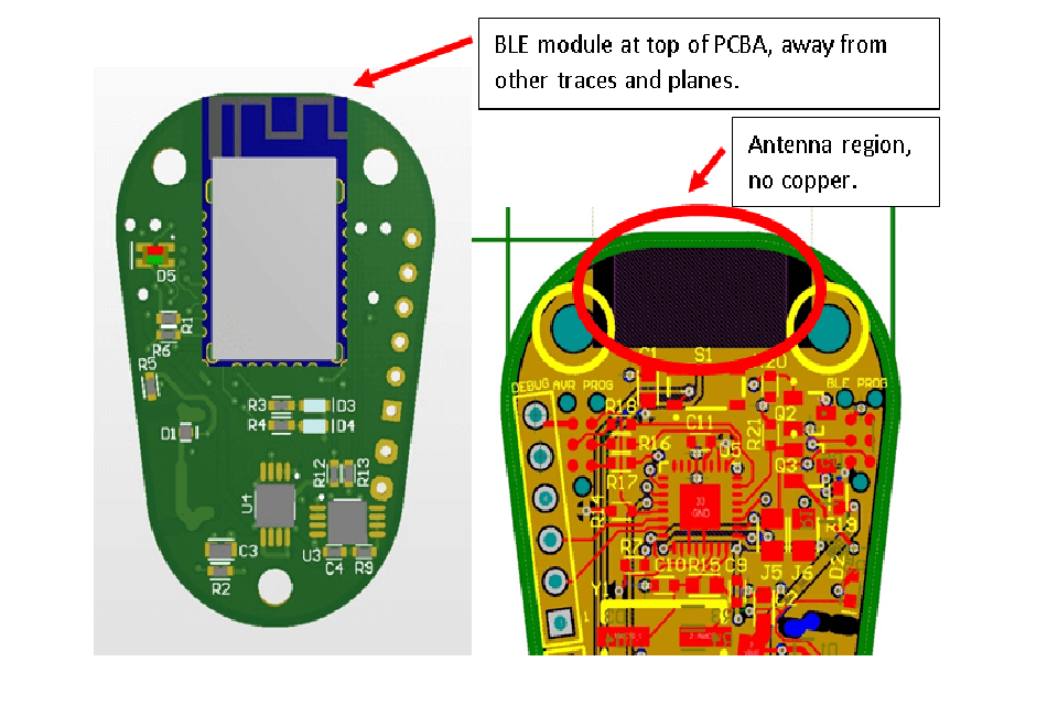
Primarily is the antenna style and positioning . The antenna is the entrance to the wireless world. Designers can use a chip antenna, a PCB trace antenna, or an external antenna. The PCB trace antenna is economical but requires very precise design and impedance matching (usually to 50 ohms) to radiate power efficiently. The location around the antenna must be kept clear of ground airplanes, elements, and metal enclosures to avoid signal detuning and blockage. Appropriate antenna tuning is vital to match the antenna’s performance to the 2.4 GHz frequency.
Second, the RF design is essential. The trace linking the Bluetooth SoC to the antenna need to be as short and direct as possible. It needs to be developed as a controlled-impedance transmission line. A solid ground plane directly under the RF circuitry and SoC assists to shield against noise and provides a steady return path for signals. The placement of other parts, specifically high-frequency digital elements like crystals or changing power supplies, should be managed carefully to avoid them from radiating sound that might disrupt the sensitive Bluetooth receiver. Utilizing strategies like protecting and proper power supply decoupling is basic practice for a robust Bluetooth PCB design.
Which Industries Greatly Rely on Bluetooth PCB Technology?
The flexibility of the modern-day Bluetooth PCB has actually driven its adoption throughout a large spectrum of markets, far beyond customer electronics. Bluetooth in each region leads to special characteristics of technology, to resolve different obstacles and produce brand-new values, from the large-scale BLE nature of Aries in each region. These applications are changing how services run and how we communicate with the world around us.
In the Smart Structures and Home Automation sector, Bluetooth Mesh is the star. A Bluetooth PCB is embedded in light fixtures, thermostats, door locks and occupancy sensing units. These nodes create a building-wide Aries network that enables the sophisticated, automated control and A/C systems to save energy.. It likewise enhances security and provides a platform for indoor navigation services. In the Industrial IoT (IIoT) , producers utilize BLE for property tracking and condition tracking. BLE tags connected to tools, equipment, and inventory transmit their location, permitting real-time tracking within a factory. Sensing units with a Bluetooth PCB monitor the vibration and temperature of equipment, predicting maintenance requirements before a failure takes place.
The Healthcare and Medical field relies heavily on the low-power and safe and secure nature of BLE. Wearable health displays, such as glucose meters, ECG spots, and pulse oximeters, use a Bluetooth PCB to transmit vital information to a mobile phone or a central monitoring station. This enables constant, remote patient monitoring.In retail, Bluetooth beacon is used for closeness marketing and customer engagement. As a consumer walking through a shop, beacons can set notice on their phone about special offers or item information, increasing shopping experience.
Table 2: Key Applications of Bluetooth PCB by Market .
| Industry | Primary Technology Used | Example Applications | Key Benefit |
|---|---|---|---|
| Customer Electronic devices | Bluetooth Classic, BLE | Wireless headphones, speakers, smartwatches, physical fitness trackers | Convenience, Cable Replacement |
| Smart Structures | Bluetooth Mesh, BLE | Smart lighting, heating and cooling control, access control, tenancy picking up | Energy Performance, Centralized Control |
| Industrial IoT (IIoT) | BLE, Bluetooth Mesh | Possession tracking, predictive maintenance, procedure tracking | Functional Efficiency, Safety |
| Health care | BLE | Remote patient screens, connected medical gadgets, senior care | Enhanced Patient Outcomes, Information Gain Access To |
| Retail | BLE (Beacons) | Distance marketing, indoor navigation, property tracking | Enhanced Client Experience |
| Smart Cities | Bluetooth Mesh, BLE | Smart street lighting, public transit tracking, ecological noticing | Public Safety, Resource Management |
How is Web Bluetooth Shaping Future Gadget Interaction?
Web Bluetooth is a forward-looking API (Application Shows Interface) that intends to bridge the space in between the web browser and physical Bluetooth gadgets. Developed by engineers at Google, this basic enables a websites running in a compatible browser (like Chrome) to straight find, connect to, and control nearby BLE gadgets. This eliminates a substantial point of friction for users: the need to download and set up a devoted native mobile application for every single Bluetooth gizmo they own.
The ramifications of this are significant. Imagine a scenario where you buy a new set of clever scales. Instead of going to an app shop, you might merely navigate to the producer’s site. The site might then use the Web Bluetooth API to discover your scales, link to them, and show your weight and body composition information straight in the web browser. This structured experience reduces the barrier to entry for users and streamlines advancement for makers, who can focus on developing a single web application rather of separate apps for iOS and Android.
For designers working with a Bluetooth PCB , Web Bluetooth provides a brand-new, effective channel for gadget interaction. The gadget’s firmware must be developed to interact utilizing standard BLE GATT (Generic Attribute Profile) services and characteristics, which the web browser can then translate. While still an emerging technology and not yet generally supported by all browsers, Web Bluetooth indicate a future where interaction with the IoT is more seamless and incorporated directly into the web, further broadening the reach and energy of every Bluetooth PCB – made it possible for gadget.
How Do You Select the Right Bluetooth Module for Your PCB Project?
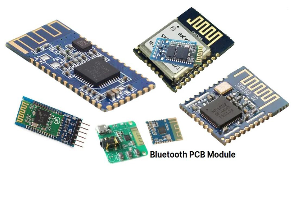
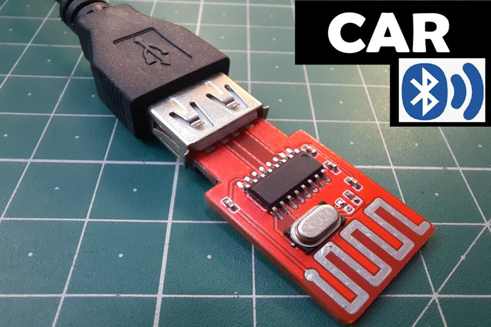
Choosing the proper Bluetooth component is one of the most vital decisions in the item development lifecycle. The choice largely boils down to utilizing a pre-certified Bluetooth module versus developing a custom-made service with a raw Bluetooth chip (SoC) . Each technique has unique compromises in regards to expense, time-to-market, and design flexibility.
A Bluetooth module is a small, self-contained PCB that consists of the Bluetooth SoC, antenna, and all essential supporting components. These modules are attractive because they are pre-certified by regulatory bodies like the FCC (in the United States) and CE (in Europe). This allows a business to bypass the expensive and lengthy procedure of RF testing and certification, significantly speeding up the time-to-market. Modules are perfect for start-ups, low-to-medium volume production runs, or for groups without deep in-house RF engineering expertise. The compromise is a greater per-unit cost and less flexibility in kind factor.
Alternatively, a chip-down style includes integrating the raw Bluetooth SoC straight onto your main Bluetooth PCB . This approach offers optimal style versatility, permitting you to develop the smallest possible kind aspect and optimize the design for your specific application. In too much production versions (usually more than 100,000 systems), the cost per unit of a chip is much lower than a module, which saves considerable expenditure. Nevertheless, this path requires enough RF design knowledge to manage antenna, impedance control and intervention mitigation. It also demands a full regulatory accreditation process, which includes expense and can delay item launch. The choice depends upon a mindful analysis of your job’s budget plan, timeline, volume, and in-house technical abilities.
Often Asked Questions (Frequently Asked Questions) .
1. What is the primary distinction in between a Bluetooth chip and a Bluetooth module?
A Bluetooth chip (SoC) is the raw integrated circuit that supplies Bluetooth performance. A Bluetooth module is a little, pre-built circuit board that includes the chip, antenna, and all needed parts. Modules are pre-certified, which accelerates item development, while chips offer more style versatility and lower cost at high volumes however need custom-made style and accreditation.
2.How far can a modern-day Bluetooth PCB transfer a signal? .
The range depends upon the Bluetooth variation and environment. Bluetooth classic usually has a series of about 10 meters. Bluetooth 5, using its long-range mode (coded phy), can achieve a theoretical line-of-vision chain of 400 meters, although the practical variety of 150–200 meters is more specific in real-world applications.
3. Is creating a Bluetooth PCB hard? .
Yes, it can be difficult to make a high-demonstration Bluetooth PCB. It requires special understanding in RF (radio frequency) engineering, including antenna design, impedance, and reducing sound and intervention. For teams without this knowledge, using a pre-certified Bluetooth module is frequently the suggested method.
4. Do a Bluetooth and Wi-Fi interfere with each other?
Yes, since both technologies work in the same 2.4 GHz frequency bands exactly, they can interrupt each other. However, modern Bluetooth standards include adaptive frequency hoping (AFH) and other co-existence mechanisms that intelligently spot and prevent frequencies used by Wi-Fi, much less intervention.
5. What is a “GATT Profile” in Bluetooth Low Energy? .
GATT (Generic Quality Profile) specifies the structure of how data is exchanged in BLE. It develops a hierarchy of Providers and Characteristics. A “Service” is a collection of data connected to a particular function (e.g., a “Heart Rate Service”). A “Particular” is a particular data value within that service (e.g., the “Heart Rate Measurement”). This standardized structure allows different devices to understand and interpret each other’s data.
6. Why is a “keep-out location” crucial for a PCB antenna?
The keep-out area is a designated area on the Bluetooth PCB around the antenna that need to be kept without copper aircrafts, traces, and elements. Metal in close proximity to the antenna can absorb and show radio waves, detuning the antenna and significantly deteriorating its efficiency. A correct keep-out location is important for accomplishing the device’s ranked wireless variety and reliability.
Conclusion .
The Bluetooth PCB has actually developed far beyond its origins as an easy tool for removing cables. It now stands as an essential enabler of the interconnected world assured by the Web of Things. Through ruthless development, the technology has actually adjusted to meet contemporary demands for lower power, greater variety, and more intricate network abilities. The development of Bluetooth Low Energy has opened the potential for billions of battery-powered devices, while Bluetooth Mesh has offered the framework for producing vast, smart, and dependable control networks.
From wise homes and intelligent structures to innovative industrial automation and personal health care, the Bluetooth PCB is the hidden yet important part driving development.Continuous progress, such as Bluetooth 5 and emerging web Bluetooth seen in Bluetooth standard, make sure the innovation will remain relevant and will continue to search for brand-new applications. Understanding the technical nuances of designing a Bluetooth PCB and strategic implications of its many requirements are no longer alternative; This is a condition for anyone wishing to innovate in today’s technology-operated market. The future is wireless, and it is being made, a Bluetooth PCB at a time.
Summary of Secret Points .
- A Bluetooth PCB is the core hardware that incorporates a Bluetooth radio, MCU, and antenna to allow cordless interaction.
- The innovation has actually evolved from Bluetooth Classic (cable replacement) to highly efficient and capable requirements like Bluetooth Low Energy (BLE) and Bluetooth Mesh .
- BLE is a game-changer for battery-powered IoT devices due to its incredibly low power intake.
- Bluetooth Mesh makes it possible for large-scale, many-to-many communication, perfect for wise buildings and industrial applications.
- Bluetooth 5 speeds, range (about 4X), and data broadcasting capacity provides IOT capabilities.
- Critical Bluetooth PCB style aspects consist of precise antenna design, impedance matching, and a tidy RF layout to avoid disturbance.
- The choice between a pre-certified module and a chip-down style depends upon volume, expense, time-to-market, and engineering proficiency.
- The marketplace for Bluetooth gadgets is experiencing enormous growth, driven largely by the adoption of BLE in diverse markets.
.