The Core Function of Security PCB Assembly in Security Systems
Article Summary
The structure of any modern security system– from a high-definition monitoring electronic camera to an advanced gain access to control panel– is not the software application or the casing, but the electronic devices within. At the heart of these electronic devices lies the security PCB assembly . This detailed process of mounting electronic elements onto a printed circuit board (PCB) dictates the system’s reliability, efficiency, and intelligence. This post offers a detailed, technical deep-dive into the important world of security PCB assembly , exploring the advanced processes, materials, and design factors to consider that empower today’s security innovation. We will dissect how these assemblies work in core applications and what future innovations, like 5G and edge AI, hold for the market.
Table of Contents
Abstract
This post provides an in-depth analysis of security PCB assembly (PCBA) , recognizing it as the fundamental technology for modern security applications. It investigates the particular PCBA requirements for video monitoring, network video recorders (NVRs), and Web of Things (IoT) security devices. The text examines sophisticated production methods, including High-Density Interconnect (HDI) , multilayer board fabrication, and specialized surface area finishes critical for reliability. It resolves technical obstacles such as signal stability, thermal management, and electro-magnetic compatibility (EMC). Furthermore, the combination of emerging innovations like 5G and edge expert system (AI) into PCBA style is explored. The post concludes by going over future patterns towards sustainable and modular styles, providing a technical roadmap for engineers, designers, and manufacturers in the security industry.
What Exactly Is Security PCB Assembly?
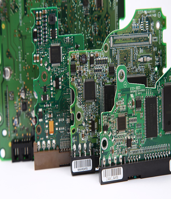
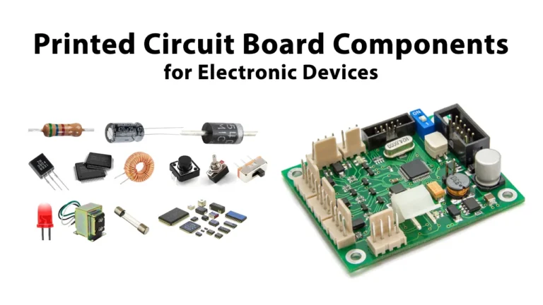
At its core, a Printed Circuit Board (PCB) is a bare board that mechanically supports and electrically connects electronic components using conductive tracks, pads, and other features. However, a bare PCB is inert. The procedure that changes it into a functional electronic brain is PCB Assembly (PCBA) . This includes sourcing parts (like microprocessors, memory, and sensors), positioning them onto the PCB using approaches like Surface-Mount Technology (SMT) or Through-Hole Technology (THT) , and soldering them completely in location.
What identifies security PCB assembly is the extreme emphasis on reliability, longevity, and efficiency under demanding conditions. Unlike consumer electronics, a failure in a security device is not a trouble; it is a vital vulnerability. Therefore, the assembly process for security systems includes more extensive screening, higher-grade materials, and develops crafted to resist environmental tension and tampering. It involves specialized considerations for power management, information stability, and the physical security of the parts themselves. This customized focus guarantees that a monitoring video camera or an alarm system functions flawlessly, 24/7, for years on end.
The whole lifecycle, from style to manufacturing, is geared towards risk mitigation. Engineers use Design for Manufacturability (DFM) and Style for Testability (DFT) principles to make sure the boards can be produced and validated with the greatest possible yield and accuracy. The last put together board, or PCBA, is the operational heart of the security gadget, carrying out every command from capturing video to setting off an alarm.
Why is High-Reliability Assembly Crucial for Security Devices?
The important for high dependability in security PCB assembly stems straight from the non-negotiable function of security systems: to protect assets, property, and lives. A single component failure or a malfunctioning solder joint can render a multi-thousand-dollar security network useless. For example, a malfunctioning processor on a cam’s PCBA could trigger video freezes, preventing the capture of important proof. A faulty capacitor in an access control system could lead to a door stopping working to lock, developing a substantial security breach.
High dependability is attained through a multi-faceted method. It starts with the choice of commercial or automotive-grade components that operate dependably across large temperature level ranges (e.g., -40 ° C to +85 ° C). The PCB substrate material itself is a crucial choice. While basic FR-4 is common, applications in extreme environments may require materials with much better thermal or high-frequency efficiency. The assembly procedure should be carefully controlled, utilizing innovations like Automated Optical Examination (AOI) and Automated X-ray Inspection (AXI) to detect microscopic problems in solder joints that might lead to future failures.
In addition, dependability reaches resisting external dangers. This consists of environmental elements like humidity and dust, for which conformal coatings are used to secure the electronics. It also includes electrical hazards like power surges and Electromagnetic Disturbance (EMI) . A robust security PCB assembly integrates detailed circuit security and follows stringent Electromagnetic Compatibility (EMC) design guidelines to guarantee the device runs predictably even in noisy electrical environments. The supreme goal is to create a device that is “install-and-forget,” functioning dependably for its entire service life without requiring frequent maintenance or intervention.
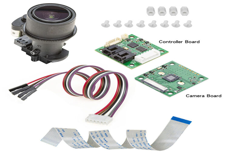
How Does Security PCB Assembly Power Video Security Systems?
Modern IP video cameras are advanced computing gadgets, and their capabilities are straight enabled by the underlying security PCB assembly . The PCBA in a high-definition cam is a dense and complicated system responsible for several concurrent tasks. At its center is frequently a powerful System on a Chip (SoC) that integrates the primary processor, memory controllers, and specialized hardware accelerators for video encoding and image processing. The assembly needs to offer this SoC with steady power and help with high-speed communication with other key elements.
One primary function is image acquisition and processing. The PCBA supplies the user interface to the CMOS image sensor, managing the high-speed data lanes that carry the raw video feed. Onboard digital signal processors (DSPs) or the SoC itself then carry out complex algorithms for functions like Wide Dynamic Range (WDR) , which balances light and dark locations of a scene, and 3D sound decrease. These processes are computationally intensive and need a PCBA created for exceptional signal integrity to prevent information corruption.
Another vital function is video compression and network transmission. The security PCB assembly hosts the hardware encoder that compresses raw video into standard formats like H. 265 or the newer H. 265+. This drastically reduces bandwidth and storage requirements. The assembly also includes the network user interface controller (NIC) and PHY chip, allowing connection to the network by means of Ethernet. For cameras with Power over Ethernet (PoE), the PCBA incorporates the essential circuitry to get power over the same cable television, simplifying setup. Each of these functions depends upon a thoroughly created and assembled circuit board.
What Role Does security PCB assembly Play in Intelligent Storage and NVRs?
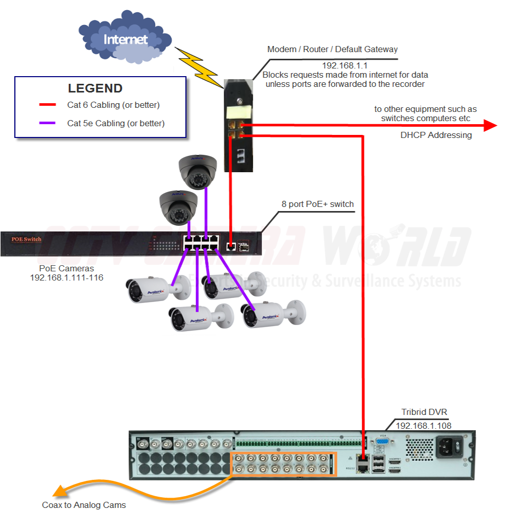
A Network Video Recorder (NVR) serves as the main brain for a monitoring network, accountable for getting, keeping, and handling video streams from numerous cams. The NVR’s motherboard is a prime example of a mission-critical security PCB assembly . Its primary function is to handle enormous information throughput dependably. The PCBA must have the ability to handle lots of high-resolution video streams concurrently, writing them to hard disk drives without dropping a single frame. This requires a high-bandwidth backplane and advanced SATA or SAS controllers incorporated straight onto the board.
Intelligent storage management is likewise a key function driven by the PCBA. The assembly hosts the primary processor that runs the NVR’s os and video management software application (VMS). This includes features like RAID (Redundant Variety of Independent Disks) management, which secures versus information loss in case of a hard disk drive failure. The PCBA style must offer robust power circulation to numerous hard disk drives and guarantee sufficient cooling, as drive failures are frequently linked to overheating.
In addition, the PCBA is the center for network connection and intelligent analytics. It incorporates Gigabit or perhaps 10-Gigabit Ethernet ports to communicate with the video camera network and user interfaces. In modern-day “AI NVRs,” the security PCB assembly may also incorporate a devoted Neural Processing Unit (NPU) or a powerful GPU. This hardware enables the NVR to carry out server-side video analytics, such as object detection, facial acknowledgment, or license plate acknowledgment, turning passive video storage into an active, smart security tool.
How is security PCB assembly Enabling the Increase of IoT Security Terminals?
The Internet of Things (IoT) has expanded the security perimeter to consist of a vast range of connected gadgets, from smart locks and video doorbells to movement sensors and automated alarm systems. The security PCB assembly for these devices presents a special set of obstacles, primarily centered around miniaturization, low power consumption, and cordless connection. Unlike a stationary NVR, many IoT security gadgets are small, battery-powered, and need to run for months or years on a single charge.
Power effectiveness is critical. The PCBA design for a battery-powered movement sensing unit, for example, should be optimized for ultra-low-power deep sleep modes. Engineers choose components, such as microcontrollers and wireless modules (e.g., LoRaWAN, Zigbee, or Wi-Fi), particularly for their low standby current intake. The assembly itself should be free of any present leak paths that might prematurely drain the battery. The PCBA’s power management integrated circuit (PMIC) plays an essential function in dynamically adjusting power delivery to various parts of the circuit, guaranteeing energy is just used when definitely essential.
In addition to power, the PCBA in an IoT terminal deals with noticing, processing, and communication. It integrates the main sensing unit (e.g., a passive infrared sensing unit for motion, or a magnetic switch for a door), a microcontroller to analyze the sensor’s data, and a radio module to send alerts wirelessly to a main center or the cloud. For advanced gadgets like clever locks, the security PCB assembly likewise integrates safe elements for cryptographic crucial storage and biometric sensor controllers, guaranteeing both physical and digital security are robustly handled at the hardware level.
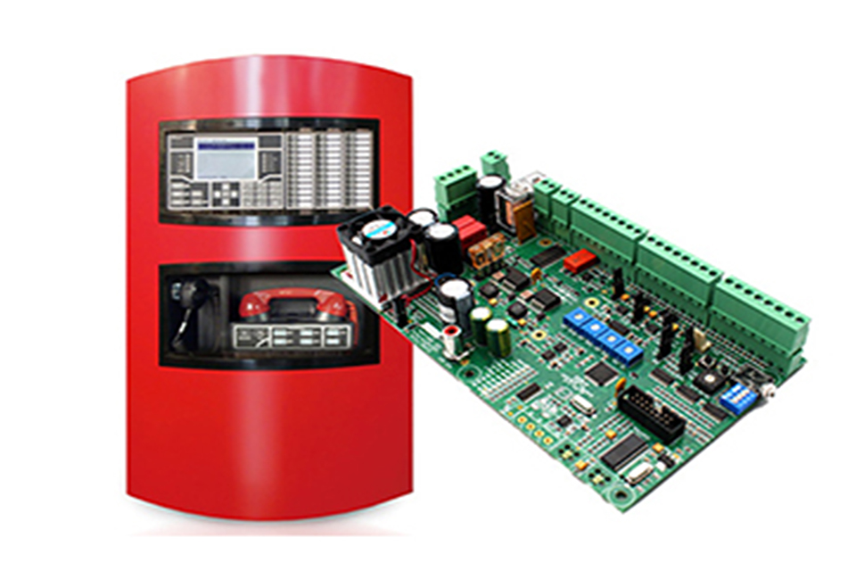
- Recommended Image: A side-by-side contrast of a large NVR motherboard and a small, compact PCBA from a wireless door sensor, showing the various style top priorities. *.
What Advanced Manufacturing Processes Define Modern Security PCBA?
The increasing intricacy and miniaturization of security devices require sophisticated production processes for their PCBAs. Standard single or double-layer boards are typically inadequate. Modern security PCB assembly depends on advanced techniques to load more performance into smaller sized spaces while keeping exceptional dependability.
One of the most essential technologies is High-Density Interconnect (HDI) . HDI PCBs feature much finer lines and spaces, smaller sized vias (laser-drilled microvias), and greater connection pad density than standard boards. This permits designers to put elements like fine-pitch Ball Grid Variety (BGA) bundles– common for effective SoCs– much closer together. Using HDI and multilayer board styles (typically 8 to 12 layers or more) is important for handling complex routing and guaranteeing signal integrity in high-speed circuits, while likewise supplying devoted ground and power airplanes to minimize electronic noise.
The choice of surface area finish is also vital for long-term dependability. While basic Hot Air Solder Leveling (HASL) is affordable, it does not offer the completely flat surface required for fine-pitch parts. For high-performance security PCB assembly , finishes like Electroless Nickel Immersion Gold (ENIG) are preferred. ENIG supplies a flat, long lasting, and corrosion-resistant surface area, ensuring excellent solderability and long-lasting joint stability, specifically in gadgets exposed to fluctuating ecological conditions. The entire procedure is a symphony of precision engineering, from solder paste application to reflow oven profiling, all customized to the particular requirements of a security application.
Table: Comparison of PCB Substrate Materials for Security Applications
| Material Type | Secret Properties | Common Security Application | Cost Factor |
|---|---|---|---|
| FR-4 (Basic) | Good insulation, mechanically strong, economical. | Indoor video cameras, access control panels, alarm. | Low |
| FR-4 (High-Tg) | Greater glass transition temperature level (> 170 ° C). Resists deformation under heat. | Outside video cameras in hot climates, NVRs with high power density. | Medium |
| Rogers Material | Exceptional high-frequency efficiency (low dielectric loss). | 5G-enabled security gadgets, high-frequency radar sensing units. | High |
| Metal-Core PCB (MCPCB) | Aluminum or copper base for remarkable thermal dissipation. | High-power infrared (IR) LED varieties for night vision video cameras. | Medium-High |
How Do We Overcome Secret Technical Obstacles in Security PCB Assembly?
Designing and making a flawless security PCB assembly includes navigating a minefield of prospective technical problems. Three of the most significant obstacles are signal integrity, thermal management, and electromagnetic compatibility. Proactively addressing these during the style stage is essential for an effective product.
Signal Stability (SI) becomes a significant concern as processing speeds and information rates increase. In a security electronic camera streaming 4K video, high-speed signals can deteriorate, show, or hinder each other (crosstalk), leading to data mistakes or system crashes. Engineers utilize advanced simulation software application to create regulated impedance traces, guaranteeing signals propagate easily. Techniques like precise trace length matching for differential sets (e.g., for USB or Ethernet) and strategic placement of elements are used throughout the PCB layout stage to maintain signal quality on the final put together board.
Thermal Management is another important obstacle, specifically in fanless devices like many contemporary security video cameras or compact NVRs. High-performance processors and PoE modules can create considerable heat. If not dissipated efficiently, this heat can cause part failure and drastically shorten the device’s life-span. Solutions embedded in the security PCB assembly consist of utilizing thermal vias to draw heat from an element to a large ground aircraft or a metal chassis, increasing the copper weight (density) of power airplanes, and utilizing Metal-Core PCBs for parts like high-power LEDs. 3D thermal simulation is typically utilized to model heat flow and optimize the layout before any physical prototypes are constructed.
Electromagnetic Compatibility (EMC) guarantees a device does not emit extreme electromagnetic disturbance (EMI) and is not susceptible to EMI from external sources. A security device that fails EMC screening can not be legally offered in most parts of the world (e.g., it must pass FCC Class B in the United States). A well-designed PCBA for security applications will incorporate comprehensive filtering on power and signal lines, proper grounding and protecting, and a multilayer stack-up that isolates loud digital circuits from delicate analog ones.
What Methods Can Manage the Costs of High-Security PCB Assembly?
While dependability is vital, expense is constantly a useful consideration. The goal is to attain the needed efficiency and reliability without over-engineering the product. A smart security PCB assembly strategy balances these elements through numerous essential approaches. The most impactful is Style for Manufacturability (DFM) and the more comprehensive Style for Quality (DFX) , which includes design for assembly, testing, and supply chain.
DFM includes creating the PCBA in such a way that lines up with the capabilities of the selected assembly partner. This includes utilizing basic element sizes and footprints where possible, providing appropriate spacing between parts to accommodate assembly machinery, and creating clear fiducial markers and test points. Following DFM guidelines substantially minimizes the danger of manufacturing flaws, which in turn increases production yield and reduces the per-unit expense. A single style modification caught by a DFM check can save thousands of dollars in ditched boards and rework.
Another effective method is modular style . Instead of producing a completely distinct PCBA for every item variant, engineers can create a universal primary board that contains the core processing and I/O. Product-specific features can then be added via smaller sized, less expensive plug-in modules. For example, a cam platform may utilize the exact same core security PCB assembly for all designs, with different sensor modules or network modules (e.g., Wi-Fi vs. cellular) being the only variable. This method drastically lowers non-recurring engineering (NRE) costs, streamlines stock management, and accelerates time-to-market for brand-new item variations.
How Will 5G and Edge AI Reshape Security Circuit Board Style?
The next generation of security innovation is being driven by the merging of 5G and Artificial Intelligence at the edge. These patterns place brand-new and requiring requirements on security PCB assembly . The shift to 5G, with its guarantee of ultra-low latency and high bandwidth, requires a complete overhaul of the radio frequency (RF) section of a circuit board.
5G runs at much higher frequencies than previous cellular innovations. This requires using specialized PCB materials (like Rogers or comparable low-loss dielectrics) to avoid signal deterioration. The PCBA design should integrate sophisticated RF front-end modules and thoroughly developed antenna systems. Protecting becomes much more important to avoid the 5G radio from interfering with the rest of the delicate electronic devices on the board. The layout of these boards is a complicated art, requiring expertise in both high-speed digital and high-frequency RF design.
5G runs at much greater frequencies than previous cellular technologies. This demands the use of specialized PCB materials (like Rogers or comparable low-loss dielectrics) to avoid signal deterioration. The PCBA design must integrate advanced RF front-end modules and thoroughly created antenna systems. Protecting ends up being even more crucial to avoid the 5G radio from hindering the rest of the delicate electronic devices on the board. The layout of these boards is an intricate art, requiring proficiency in both high-speed digital and high-frequency RF style.
At the same time, Edge AI is moving processing from the cloud or NVR directly onto the device itself. This is enabled by integrating dedicated Neural Processing Units (NPUs) or AI accelerators into the gadget’s SoC. This allows a camera to perform complicated analytics like real-time things category or habits analysis in your area. For the security PCB assembly , this suggests accommodating more powerful processors that consume more power and create more heat. It requires advanced power management architectures, like Bundle on Package (PoP) assembly to stack memory on top of the processor for a smaller footprint, and more robust thermal management solutions to keep these powerful chips running within their safe temperature limits.
What Does a Sustainable and Future-Proof Security PCBA Look Like?
Beyond instant performance, the industry is significantly concentrated on sustainability and long-lasting viability. A future-proof security PCB assembly must consider its entire lifecycle, from material sourcing to end-of-life disposal. This starts with compliance with environmental regulations like the Restriction of Hazardous Compounds (RoHS) directive, which restricts using materials like lead, mercury, and cadmium. Accountable manufacturers make sure 100% of their parts and procedures are RoHS certified.
Sustainability likewise reaches the supply chain. This consists of ethical sourcing of minerals (in line with guidelines regarding “dispute minerals” like tin, tungsten, and gold) and building resilient supply chains that can withstand interruptions, such as the global chip lacks. A forward-thinking method involves designing PCBAs that can accept alternative parts from different manufacturers without requiring a total redesign, providing important versatility.
Finally, a sustainable and future-proof style is a modular one. Designing for repairability and upgradability is a crucial element. For instance, if a network user interface stops working, a modular style would permit the replacement of simply that little module, rather than the entire costly motherboard. This not only minimizes electronic waste but also lowers the overall cost of ownership for the end-user. The most innovative security PCB assembly methods are not just about creating a powerful device for today, but a responsible and versatile platform for tomorrow.
FAQ
Q1: How does security PCB assembly deal with operation in severe high-temperature environments?
It uses a multi-pronged strategy. Initially, designers select high-temperature-grade products like High-Tg FR-4 or specialized substrates that withstand warping. Second, they use elements with industrial or automotive temperature level rankings (-40 ° C to +85 ° C or higher ). Third, the PCB design integrates thermal management methods like big copper aircrafts, thermal vias to link to a heat sink, and the possible usage of Metal-Core PCBs (MCPCBs) for very high-heat elements like IR LEDs.
Q2: What is the specific role of the PCBA in a modern-day smart gain access to control system?
In a smart access control system, the PCBA is the central nervous system. It processes biometric data from fingerprint or facial scanners, performs cryptographic functions to confirm qualifications, and drives the electric lock mechanism. It likewise incorporates numerous communication procedures (e.g., Wiegand, OSDP, Ethernet, Wi-Fi) to communicate safely with a central server and provides robust power management and backup battery circuit control.
Q3: How do you ensure the long-term reliability of a security PCBA in a damp or destructive environment? .
The main defense is the application of a conformal finish . This is a thin, protective polymer movie that is applied over the finished PCBA, sealing the elements and solder joints from moisture, dust, and chemicals. Furthermore, designers specify corrosion-resistant PCB surface finishes like ENIG (Electroless Nickel Immersion Gold) and use sealed or hermetic elements where essential to avoid ingress.
Q4: What are the primary effects of 5G innovation on the style and assembly of a security PCB
5G integration introduces substantial RF/microwave style obstacles. The PCBA should use low-loss dielectric products to manage high frequencies. It needs meticulous layout for the 5G module and its antennas to guarantee signal integrity and avoid disturbance with other digital components. Boosted EMC/EMI protecting is crucial, and the power shipment network need to be robust enough to deal with the greater power demands of the 5G radio during transmission.
Q5: How is the power consumption of a PCBA enhanced in a battery-powered smart tracking system?
Optimization is achieved through both software and hardware. The security PCB assembly uses ultra-low-power microcontrollers and components. The power management integrated circuit (PMIC) is vital, enabling vibrant voltage scaling and the ability to shut down power to unused sections of the board. The firmware then carries out aggressive sleep modes, waking the device just when an event is activated by a sensing unit, which decreases active time and extends battery life from weeks to years.
Q6: What are the vital assessment and screening actions in a high-reliability security PCB assembly procedure?
An extensive evaluation process includes a number of stages. Automated Optical Evaluation (AOI) utilizes cameras to check for placement errors and noticeable solder defects. Automated X-ray Examination (AXI) is used to check surprise solder joints, such as those under Ball Grid Array (BGA) parts. This is followed by In-Circuit Screening (ICT) to inspect electrical connections and an initial Practical Test (FCT) to confirm the board operates as designed. Finally, numerous security items go through an aging or burn-in test , where they are operated under stress (e.g., heat) for an extended duration to capture early-life failures.
Conclusion
The security PCB assembly is even more than a simple collection of parts on a board; it is the extremely engineered and rigorously evaluated technological core that dictates the performance, intelligence, and– most notably– the dependability of every contemporary security system. From the high-speed data processing in a 4K cam to the low-power caution of a remote IoT sensing unit, the capabilities of the device are directly born from the quality of its PCBA.
As the industry advances towards the combination of 5G, edge AI, and more advanced analytics, the needs on PCBA style and production will just intensify. Success will come from those who master the intricacies of high-density style, thermal management, signal stability, and robust production processes. By focusing on reliability, adopting modular and sustainable design concepts, and embracing new innovations, the field of security PCB assembly will continue to be the quiet, vital hero powering a much safer, more protected world.
Summary of Secret Points to Remember
- Foundation of Trust: Security PCB assembly is the vital procedure that figures out a security gadget’s reliability. A failure here is a security breach.
- Application-Specific Design: The PCBA for a cam, NVR, or IoT sensor has vastly different requirements for power, processing, and connectivity.
- Advanced Production is Secret: Technologies like HDI, multilayer boards, and ENIG surface finishes are not optional luxuries; they are important for modern-day, compact, high-performance security gadgets.
- Overcoming Challenges: Proactive style to handle signal integrity, heat, and electro-magnetic interference is non-negotiable for creating a robust product.
- Balancing Cost and Quality: Smart techniques like DFM and modular style enable affordable production without compromising the high reliability needed for security applications.
- The Future is Integrated: The next frontier of security PCB assembly includes incorporating 5G and edge AI, which requires new materials, advanced thermal solutions, and advanced RF style expertise.
- Sustainability Matters: Future-proof design includes RoHS compliance, ethical sourcing, and modularity for repair work and upgrades, decreasing e-waste and total cost of ownership.