Precision Watch LED PCB Board Assembly Strategies
Abstract
This article explores the detailed domain of See LED PCB board assembly . It explores the important style factors to consider, producing processes, and quality control protocols essential for producing high-performance Printed Circuit Boards (PCBs) for contemporary wrist watches including LED screens. We examine the distinct obstacles posed by miniaturization, power effectiveness, and signal integrity in wearable technology. Furthermore, the discussion encompasses related sophisticated PCB innovations, such as those for solar-powered RGB LED systems and flexible rigid-flex circuits, highlighting the transferable knowledge in precision electronics manufacturing. The objective is to provide an extensive understanding of the technologies and approaches that underpin trusted and efficient View LED PCB board assembly .
Table of Contents
Intro
The evolution of personal electronic devices has actually regularly trended towards miniaturization and enhanced performance. Nowhere is this more apparent than in wearable innovation, particularly smartwatches and advanced digital timepieces. At the heart of these devices lies the Printed Circuit Board (PCB), an engineering marvel that hosts and interconnects all electronic elements. When these watches include Light Emitting Diodes (LEDs) for screen or lighting, the complexity of the View LED PCB board assembly procedure increases significantly. This assembly demands extraordinary precision, specialized knowledge, and advanced manufacturing capabilities.
This document supplies a scientific and technological expedition of Watch LED PCB board assembly . We will dissect the critical elements, from preliminary design factors to consider customized for compact kind aspects to the precise assembly procedures and strenuous testing procedures. Comprehending these aspects is essential for producers aiming to produce trusted, resilient, and high-performing LED-equipped watches. We will also discuss analogous PCB innovations, such as those for solar-powered lighting and rigid-flex applications, to illustrate the breadth of competence required in contemporary electronics making. The focus remains on active voice and clear, succinct descriptions to brighten this specialized field.
1. Fundamental Concepts of Watch LED PCB Board Assembly
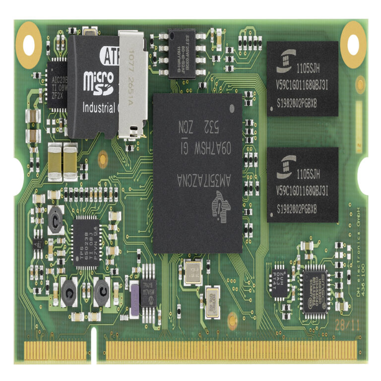
The assembly of a See LED PCB board assembly is a multi-stage process that integrates style resourcefulness with producing precision. A PCB acts as the mechanical assistance and electrical connection foundation for electronic elements using conductive tracks, pads, and other functions engraved from copper sheets laminated onto a non-conductive substrate. For watches, particularly those with LED screens, a number of aspects become vital:.
- Miniaturization: Watch casings provide exceptionally minimal space. PCB designers must make use of innovative methods like High-Density Interconnect (HDI) to accommodate all needed elements.
- Power Efficiency: Battery life is a crucial user issue. The PCB design and component choice need to minimize power consumption, particularly for the LED display screen and associated driver circuitry.
- Signal Stability: High-frequency signals for processors, memory, and interaction modules (like Bluetooth) must be managed thoroughly to avoid interference and guarantee reputable operation.
- Thermal Management: LEDs, even small ones, produce heat. The PCB should assist dissipate this heat to prevent part damage and keep efficiency.
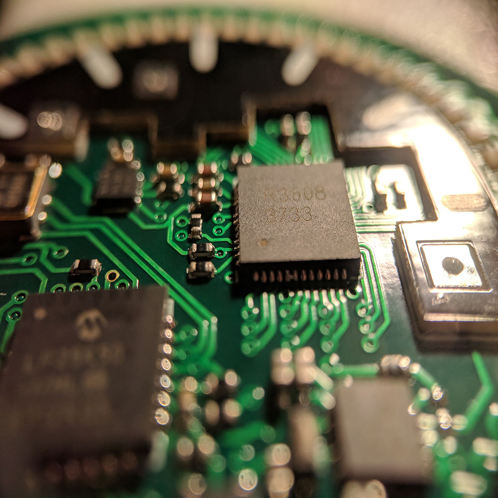
The Enjoy LED PCB board assembly process itself includes precisely positioning and soldering tiny Surface Mount Gadget (SMDs), including the LEDs, microcontrollers, sensors, and power management ICs, onto the PCB.
2. Key Parts in Watch LED PCB board assembly Systems
A normal View LED PCB board assembly will host a range of vital components, each playing a vital function:.
- Microcontroller System (MCU): The “brain” of the watch, managing all functions, including driving the LED display.
- LEDs and LED Chauffeurs: The light-emitting diodes for the display and specialized ICs (drivers) that manage their brightness and activation. These can range from simple sector LEDs to micro-LED arrays for high-resolution display screens.
- Sensing units: Accelerometers, gyroscopes, heart rate screens, and GPS modules prevail in smartwatches. Their integration onto the PCB needs careful layout.
- Power Management IC (PMIC): Handles battery charging, power distribution, and voltage regulation, important for enhancing battery life.
- Memory: Flash memory for firmware and user data, and RAM for operational processes.
- Connectivity Modules: Bluetooth, Wi-Fi, NFC chips and their associated antennas. Antenna style and placement are vital for efficiency.
- Passive Parts: Resistors, capacitors, inductors in mini packages (e.g., 0201, 01005 sizes) are vital for circuit tuning and stability.
3. Design Factors To Consider for Watch LED PCB Board Assembly
Achieving ideal efficiency in a View LED PCB board assembly requires precise style. Engineers concentrate on numerous crucial locations:.
3.1. Compact Style for Wearable Kind Factors . Smartwatches and modern-day LED watches demand PCBs that are extremely small and often shaped to fit non-rectangular casings.
- High-Density Interconnect (HDI) PCBs: We employ HDI innovation, which features finer lines and areas, smaller vias (microvias), and greater connection pad density. This permits more parts in a smaller sized location.
- Component Choice: Designers select the smallest readily available component bundles (e.g., 01005 passives, Wafer Level Chip Scale Packages – WLCSP) without compromising efficiency.
- Layer Stacking: Multi-layer PCBs (often 6-10 layers or more for smartwatches) are standard. The strategic arrangement of layers for power, ground, and signal routing is vital for both density and signal integrity.
3.2. Boosted Connection for Smart Includes . Modern watches are communication hubs. The Watch LED PCB board assembly should support robust cordless interaction.
- Antenna Combination: Creating and incorporating antennas (Bluetooth, Wi-Fi, GPS, NFC) straight onto the PCB or accommodating miniature chip antennas requires specialized RF (Radio Frequency) engineering knowledge. Ground aircraft style and component positioning near antennas considerably impact performance.
- Signal Seclusion: RF signals are sensitive to noise. PCB layout methods, such as guard traces and careful routing, isolate these signals from loud digital elements to ensure steady connections and avoid desensitization.
- Low Power Interaction Protocols: Designers leverage low-energy variations of interaction protocols (e.g., Bluetooth Low Energy – BLE) to minimize power drain during information transmission and idle states.
3.3. Power Management and Efficiency . Battery durability is a primary concern for any wearable device.
- Low-Power MCUs and Elements: Selecting components created for low-power operation is the initial step.
- Effective Power Delivery Network (PDN): The PCB’s PDN must provide clean and stable power to all elements with very little loss. This includes careful trace sizing, decoupling capacitor placement, and low-dropout regulators.
- LED Driving Efficiency: For View LED PCB board assembly , the technique of driving LEDs (e.g., direct drive vs. matrix attending to, PWM for brightness control) directly impacts power intake. Effective LED chauffeur ICs are vital.
3.4. Thermal Management Techniques . LEDs produce heat, and in a compact watch, this heat needs to be handled successfully.
- Thermal Vias: Positioning vias directly under heat-generating components (like the MCU or LED driver) allows heat to perform to inner ground or power airplanes, which function as small heatsinks.
- Copper Pours: Making use of big copper locations on the PCB surface and inner layers assists spread heat more equally.
- Part Placement: Strategically placing high-power elements far from thermally sensitive ones can enhance total reliability.
4. The Watch LED PCB Board Assembly Process
The real assembly is a high-precision operation. Here’s a streamlined breakdown:.
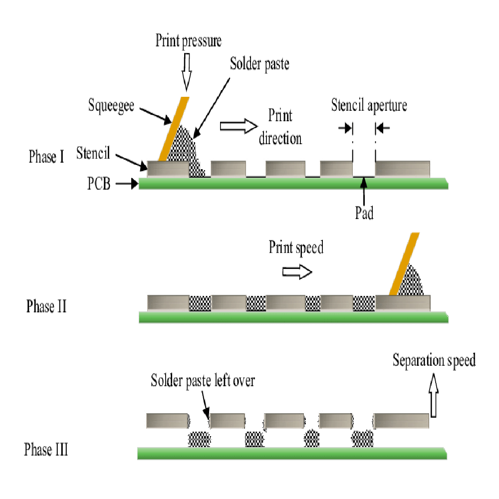
- Solder Paste Application: A stencil, precisely lined up with the PCB pads, receives solder paste. A squeegee blade presses the paste through the stencil’s apertures onto the PCB. The precision of this action is vital for good solder joints, particularly with fine-pitch components common in Enjoy LED PCB board assembly .
- Part Placement (Pick-and-Place): Automated devices choose components from reels or trays and position them onto their designated positions on the PCB with unbelievable speed and precision (typically within microns). Vision systems verify component orientation and placement.
- Reflow Soldering: The PCB, now occupied with parts held by the tacky solder paste, passes through a reflow oven. The oven has several zones with specifically controlled temperature level profiles that melt the solder, forming long-term electrical connections. The profile must be optimized for the particular parts and PCB products.
- Examination (Automated Optical Evaluation – AOI): After reflow, an AOI system utilizes electronic cameras to scan the PCB for placement errors, soldering problems (shorts, opens, inadequate solder), and incorrect part polarity. This is a vital step in View LED PCB board assembly due to the high component density.
- Wave Soldering or Selective Soldering (for THCs): If through-hole components are present, they are soldered utilizing wave soldering (for mass soldering) or selective soldering (for specific points).
- Cleaning: Flux residues from soldering can be corrosive or cause electrical issues over time. PCBs undergo a cleaning process using specialized solvents or aqueous solutions.
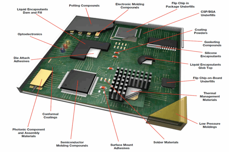
- Conformal Coating (Optional but Recommended): For enhanced durability and moisture resistance, a thin layer of non-conductive conformal coating can be applied over the assembled PCB. This is particularly beneficial for wearables exposed to sweat or occasional splashes.5. Expanding Knowledge: Solar RGB LED Light Circuit Boards .
While distinct from watch applications, the expertise gotten in accuracy PCB production is transferable to other requiring fields, such as solar-powered RGB LED lighting. These systems require robust and efficient circuit boards.
5.1. Effective Illumination with Energy Cost Savings
Solar RGB LED lights are popular for outdoor and decorative illumination. Their circuit boards need to:.
- Take Full Advantage Of Energy Effectiveness: Transform solar energy into light with very little loss. High-efficiency LED drivers and power conversion circuits are key. We design these to minimize energy usage while delivering lively, premium light.
- Color Control: Manage numerous RGB LED channels to produce a wide spectrum of colors and dynamic lighting results. This includes exact control signals from the MCU.
5.2. Seamless Combination with Solar Panels . Efficient energy harvesting and storage are crucial.
- MPPT Controllers: Our circuit boards for solar applications often include Optimum Power Point Tracking (MPPT) controllers. These gadgets enhance the power extracted from the photovoltaic panel under differing sunlight conditions, substantially enhancing charging effectiveness.
- Battery Management Systems (BMS): For systems with rechargeable batteries, a BMS on the PCB protects the battery from overcharging, over-discharging, and extreme temperature levels, extending its life-span.
This capability in creating power-efficient and environmentally robust PCBs matches the abilities needed for sophisticated View LED PCB board assembly .
6. The Function of Fast Turn Rigid-Flex PCBs
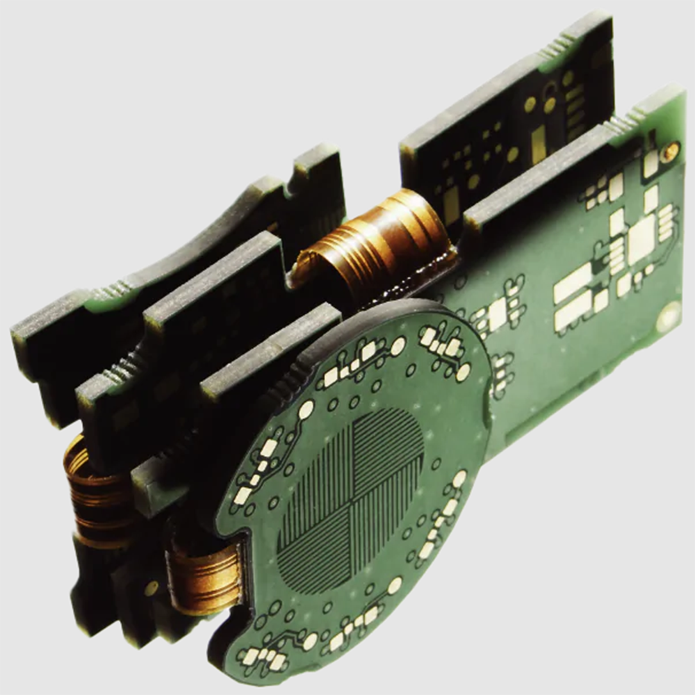
Rigid-flex PCBs offer distinct advantages in applications where area is tight, and vibrant movement or complex 3D form aspects are needed. This innovation is extremely appropriate for innovative wearable gadgets, consisting of some watch styles.
6.1. Versatile Style for Complex Requirements . Rigid-flex PCBs combine the attributes of rigid boards with the bendability of flexible circuits.
- Three-Dimensional Styles: They can be bent, folded, and shaped to suit detailed enclosures, minimizing the need for cable televisions and adapters. This is ideal for compact View LED PCB board assembly where every millimeter counts.
- Enhanced Reliability: By getting rid of connectors between stiff sections, rigid-flex styles minimize possible points of failure, improving general item dependability.
- Dynamic Flexing: In some wearable applications, the PCB may need to bend throughout usage. Rigid-flex construction can accommodate this.
6.2. Resilience for Extreme Environments . Rigid-flex PCBs, when designed with appropriate materials (like polyimide for the flex sections), can be very durable.
- Resistance to Vibration and Shock: The intrinsic flexibility can absorb mechanical tension better than simply rigid boards.
- Suitability for Wearables: This makes them appropriate for watches and other wearables that are subject to everyday motion and possible impacts. For outside solar LED systems, their ability to hold up against temperature level variations and wetness (with proper sealing and finish) is likewise a considerable advantage.
Table 1: Comparison of PCB Technologies for Miniaturized Electronics .
| Feature | Requirement Rigid PCB | Versatile PCB (FPC) | Rigid-Flex PCB | Application in Watch LED PCBs |
|---|---|---|---|---|
| Structure | Strong, non-bendable substrate | Thin, bendable substrate | Combination of rigid & flex | Requirement stiff for main board; Rigid-flex for interconnects or shaped designs |
| Bendability | None | High | Specific sections are bendable | Permits fitting into curved watch casings, links moving parts |
| Element Density | High | Lower on flex areas | High up on stiff sections | High density needed for MCUs, sensors, LEDs on stiff parts |
| Expense | Lower | Moderate | Greater | Utilized when area optimization and reliability outweigh cost |
| Durability | Great (fixed) | Good (dynamic flexing) | Exceptional (shock/vibration) | Enhances dependability by minimizing connectors/cables |
| Use Case Example | Fundamental digital watch PCB | Connecting display to main PCB | Advanced smartwatch PCB with intricate internal routing | Optimizes internal area and allows for sleeker watch designs |
7. Accuracy Manufacturing and Customization in Watch LED PCB Assembly .
Every See LED PCB board assembly job has unique requirements. We provide customized solutions customized to these needs.
7.1. Custom PCB Layouts for Distinct Designs
Our engineering group works together carefully with clients.
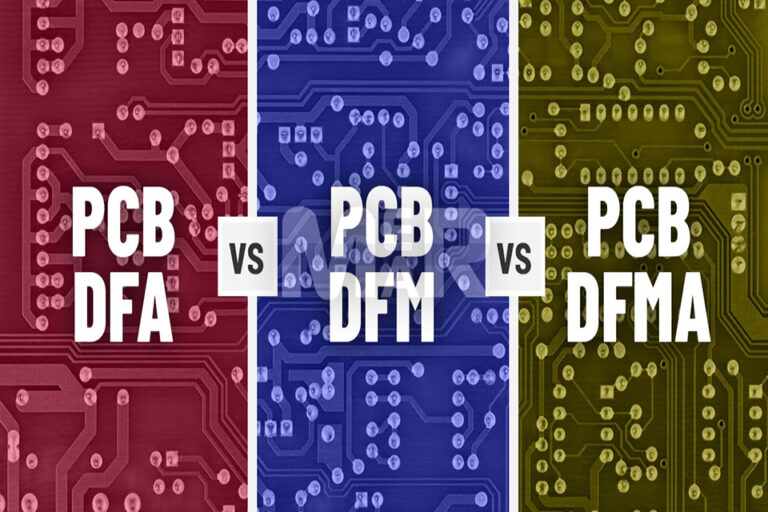
- Tailored Schematics and Layouts: We equate client specs into optimized PCB designs, considering factors like component positioning for signal integrity, thermal performance, and manufacturability (DFM – Style for Manufacturability).
- Impedance Control: For high-speed signals typical in smartwatches, accurate impedance control in PCB trace style is important. We use simulation tools and making controls to accomplish target impedances.
7.2. Quick Prototyping for Faster Time to Market . Speed is necessary in the hectic electronic devices industry.
- Fast Prototyping Solutions: We offer quick-turn prototyping for Watch LED PCB board assembly . This allows clients to validate their styles quickly, test functionality, and make required modifications before committing to mass production.
- Iterative Design: Our nimble approach supports speedy execution of design changes, minimizing advancement cycles and allowing quicker product launches.
8. Unmatched Quality Control and Testing Protocols
Quality is non-negotiable in Enjoy LED PCB board assembly . We execute extensive quality assurance throughout the manufacturing lifecycle.
- Inbound Material Assessment: All parts and bare PCBs are verified versus specifications before entering the assembly line.
- In-Process Inspection: Key stages like solder paste printing and element positioning are kept an eye on.
- Automated Optical Assessment (AOI): As mentioned, AOI checks for soldering problems, element placement mistakes, and polarity.
- X-Ray Evaluation (AXI): For intricate assemblies with Ball Grid Arrays (BGAs) or Quad Flat No-lead (QFN) bundles, where solder joints are hidden, AXI provides a non-destructive method to inspect these connections. This is vital for thick See LED PCB board assembly .
- In-Circuit Screening (ICT): ICT uses a bed-of-nails fixture to evaluate individual elements and connections on the assembled PCB, verifying shorts, opens, and proper component worths.
- Practical Evaluating (FCT): The put together PCB is powered up and evaluated for its desired functionality. For a Watch LED PCB board assembly , this would include checking LED display screen operation, sensor inputs, connection, and power usage. Custom test jigs and software application are frequently established for FCT.
- Burn-In Screening: Some assemblies might undergo burn-in screening, where they are operated under tension (e.g., elevated temperature) for a prolonged period to identify early failures.
8.1. Accreditations for Global Compliance . We abide by international quality standards.
- ISO Certification (e.g., ISO 9001): Demonstrates a dedication to quality management systems.
- RoHS Compliance: Ensures items are devoid of dangerous compounds, making them environmentally friendly and appropriate for global markets.
- IPC Standards: We follow IPC standards (e.g., IPC-A-610 for acceptability of electronic assemblies) to ensure constant quality and reliability.
9. Obstacles and Solutions in Watch LED PCB Board Assembly
The distinct demands of See LED PCB board assembly present numerous difficulties:.
- Space Restraints: .
- Challenge: * Exceptionally minimal area for parts and routing.
- Solution: * HDI innovation, microvias, multi-layer boards, element miniaturization (01005, WLCSP), and rigid-flex designs.
- Heat Dissipation: .
- Obstacle: * LEDs and MCUs create heat that can affect efficiency and durability in a confined area.
- Option: * Thermal vias, copper puts, choice of thermally efficient materials, and strategic part positioning. Advanced solutions might include miniature heat pipes or graphite spreaders in some high-end designs.
- Signal Integrity for RF and High-Speed Digital Signals: .
- Difficulty: * Crosstalk, EMI, and signal loss in dense, high-frequency environments.
- Service: * Mindful impedance control, differential pair routing, shielding, enhanced layer stack-up, and appropriate grounding methods.
- Power Effectiveness and Battery Life: .
- Difficulty: * Stabilizing functionality with user expectations for long battery life.
- Solution: * Usage of low-power components, efficient PMICs, enhanced LED driving schemes, and firmware power-saving modes.
- Fine-Pitch Part Soldering: .
- Challenge: * Increased risk of solder bridging, opens, or misalignments with really little and closely spaced component leads/pads.
- Option: * High-precision solder paste printing, advanced pick-and-place makers with vision positioning, enhanced reflow profiles, and extensive AOI/AXI assessment.
10. Future Patterns in Wearable PCB Innovation
The field of View LED PCB board assembly and wearable electronic devices is continuously evolving:.
- System-in-Package (SiP): More functions are being incorporated into single bundle modules, minimizing PCB footprint and simplifying assembly.
- Flexible and Stretchable Electronic Devices: Beyond rigid-flex, totally versatile and even stretchable PCBs could enable new type aspects for wearables that adhere completely to the body.
- Micro-LED Displays: These offer higher brightness, much better contrast, and higher power efficiency than present OLED or LCD innovations, presenting brand-new assembly challenges due to their extremely small die size.
- Advanced Materials: New substrate materials with better thermal properties, RF efficiency, or biodegradability are under research study.
- AI in Manufacturing: Artificial intelligence and machine learning are increasingly used for procedure optimization, predictive upkeep of assembly equipment, and enhanced flaw detection in AOI/AXI systems.
These patterns will continue to push the limits of View LED PCB board assembly , requiring even greater accuracy and development.
Often Asked Concerns (FAQs)
Q1: What are the main obstacles in Watch LED PCB board assembly?
The primary difficulties consist of severe miniaturization requirements, handling heat dissipation from LEDs and ICs in a confined space, guaranteeing signal integrity for high-frequency and RF signals, enhancing power efficiency for prolonged battery life, and properly soldering really fine-pitch elements.
Q2: How does High-Density Interconnect (HDI) technology benefit Enjoy LED pcb board assembly
HDI technology allows for finer conductive lines and areas, smaller sized vias (microvias), and a higher density of parts. This is crucial for watch PCBs as it allows more functionality to be packed into the very limited area available, resulting in smaller sized and sleeker watch designs.
Q3: What quality control steps are necessary for reputable Watch LED PCB board assembly? .
Essential QC steps consist of Automated Optical Examination (AOI) for solder joint and part positioning flaws, X-Ray Assessment (AXI) for surprise joints (like BGAs), In-Circuit Testing (ICT) for electrical continuity and part values, and Functional Checking (FCT) to ensure the entire assembly operates as planned. Adherence to IPC standards is likewise vital.
Q4: Why is thermal management crucial for Watch LED pcb board assembly ?
LEDs, along with the main processor (MCU) and power management ICs, produce heat. In a compact watch enclosure, this heat can develop, possibly destructive elements, lowering LED life-span, affecting performance, or triggering discomfort to the wearer. Effective thermal management (e.g., thermal vias, copper pours) dissipates this heat, guaranteeing reliability and user comfort.
Q5: Can rigid-flex PCBs be used in Watch LED PCB board assembly, and what are their benefits?
Yes, rigid-flex PCBs are progressively utilized. Their benefits include the ability to suit complex, non-flat watch case geometries, reduction in ports and cable televisions (enhancing reliability and conserving space), and much better shock/vibration resistance. They are perfect for linking different stiff areas within a watch in a compact and resilient manner.
Q6: How is power effectiveness addressed in the design and assembly of Watch LED PCBs?
Power performance is addressed by choosing low-power microcontrollers and parts, using efficient LED chauffeur ICs and power management ICs (PMICs), enhancing the PCB’s power delivery network to minimize losses, using low-power communication procedures (like BLE), and carrying out power-saving modes in the watch’s firmware.
Conclusion and Summary
The effective development of modern-day LED-equipped watches hinges critically on the quality and accuracy of their View LED PCB board assembly . This customized field demands a deep understanding of electronic style principles, advanced production processes, and rigorous quality control steps. From accommodating ultra-compact designs and guaranteeing robust connection to managing power usage and thermal output, every aspect needs precise attention to detail.
We have actually checked out the core tenets of developing and putting together PCBs for watch LEDs, including the choice of appropriate components, advanced design methods like HDI, and the crucial steps in the SMT assembly procedure. In addition, we highlighted how proficiency in associated areas, such as solar RGB LED circuit boards and versatile rigid-flex PCBs, highlights a comprehensive capability in managing complex electronic assemblies. The obstacles are significant, however with advanced technologies, experienced engineering, and a commitment to quality, manufacturers can produce trustworthy and ingenious wearable gadgets that satisfy the high expectations these days’s customers. Continuous enhancement and adaptation to emerging technologies will stay key to success in the vibrant world of Watch LED PCB board assembly .