A Comprehensive Guide to Understanding the PCB Via
Abstract.
In the intricate world of multi-layer printed circuit boards (PCBs), the PCB via works as an essential component for developing vertical electrical connections. This post offers a clinical and technical exploration of the PCB through , detailing its meaning, core functions, and main categories. We analyze the various via types, consisting of through-hole, blind, and buried vias, and compare their applications and manufacturing intricacies. Moreover, this guide analyzes crucial via covering procedures and offers practical recommendations on choosing the suitable by means of for specific design requirements, ensuring a balance in between performance, density, and expense.
Table of Contents
Introduction.
As electronic gadgets become smaller and more powerful, engineers progressively rely on multi-layer Printed Circuit Boards (PCBs) to handle complex circuitry. To make this layered structure functional, a vital part is required: the PCB via . A PCB by means of — an acronym for Vertical Interconnect Access– is more than simply a simple hole. It is a specifically engineered channel that creates electrical pathways in between various layers of the PCB. Without the PCB by means of , signals, power, and ground connections could not traverse the board, rendering multi-layer styles difficult. This guide will debunk the PCB by means of , from its fundamental meaning to its advanced applications in high-density interconnect (HDI) technology.
What is a PCB Via?
A PCB through is a plated-through hole in a PCB that electrically links copper traces on different layers of the board. The procedure begins when a maker drills a small hole through the designated layers. Following this, manufacturers transfer a layer of conductive product, generally copper, onto the inner walls of the hole. This plating changes the basic drill hole into a practical electrical avenue.
This structure permits designers to route electrical signals and power between layers, which is necessary for accomplishing the high circuit density found in modern-day electronics. In essence, the PCB by means of is the primary approach for producing three-dimensional circuits on a two-dimensional production plane.
The Functional Function of a PCB Via in Modern Electronic Devices.
While the main function of a PCB via is electrical connection, its role extends into numerous vital performance areas. Modern circuit designers make use of the PCB via tactically to boost board efficiency and dependability.
- Signal Integrity: In high-speed digital circuits, an improperly designed PCB by means of can introduce signal reflections, impedance discontinuities, and other integrity issues. Conversely, a well-designed through reduces signal destruction, ensuring that information takes a trip easily in between layers.
- Power Delivery: Engineers use arrays of PCB via, typically called “by means of stitching,” to link power and ground airplanes throughout multiple layers. This technique creates a low-inductance course, which is important for stable power shipment to delicate incorporated circuits (ICs).
- Thermal Management: Particular components, like processors and power transistors, create substantial heat. Engineers strategically put thermal vias directly under these parts. These vias function as heat pipelines, moving thermal energy from the element to bigger copper airplanes or heat sinks on other layers, thus avoiding getting too hot.
Checking Out the Main Kind Of PCB Vias.
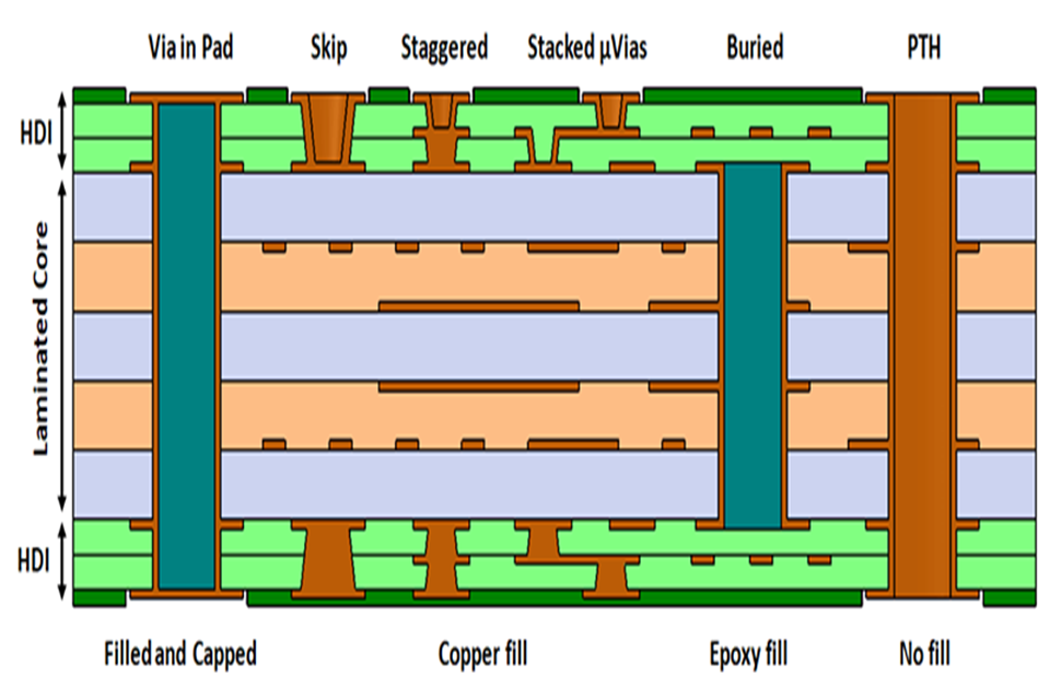
Designers categorize the PCB through based on which layers it links. This category straight impacts board complexity, density, and making cost. There are 3 primary kinds of PCB via.
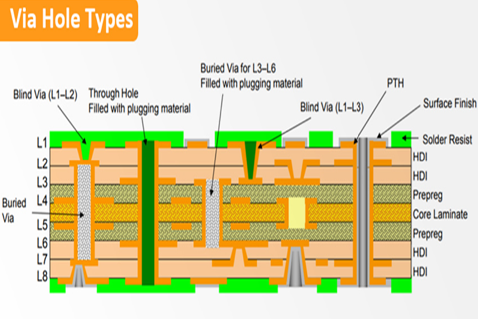
- Through-Hole Via . A through-hole by means of is the most typical and uncomplicated type. It is a hole drilled from the leading layer to the bottom layer of the PCB, travelling through all intermediate layers. Because it spans the entire board density, it can link any mix of layers. Engineers value the through-hole through for its simplicity and low production expense. They often utilize these vias for internal layer interconnections or as mounting holes for through-hole elements.
- Blind Via . A blind by means of links an external layer (top or bottom) to one or more inner layers however does not travel through the entire board. Think of a hole that starts on the surface however stops at a particular internal layer. This style maximizes important routing space on the layers listed below the endpoint of the through. The blind PCB by means of is a hallmark of High-Density Interconnect (HDI) PCBs and is often utilized in compact styles, such as those for mobile phones and wearables, specifically in Ball Grid Range (BGA) component designs.
- Buried Via . A buried by means of exists solely between two or more inner layers of a PCB. It has no connection to the external layers and is therefore totally unnoticeable from the outside of the ended up board. By linking just internal layers, a buried PCB via assists separate signals, reducing the danger of noise and interference. This makes it a perfect choice for thick, high-performance styles where signal stability is paramount. Like blind vias, the buried PCB through is an essential enabler of HDI innovation.
Comparison of PCB Via Types.
To assist clarify the differences, the table listed below compares the 3 primary PCB by means of types across several crucial qualities.
| Function | Through-Hole Via | Blind Via | Buried Via |
|---|---|---|---|
| Description | Connects top to bottom layer | Links an outer layer to an inner layer | Connects 2 or more inner layers |
| Visibility | Visible on both sides of the PCB | Noticeable on one side of the PCB | Not noticeable on the exterior |
| Board Density | Lower | Greater | Greatest |
| Production Expense | Low | High | High |
| Manufacturing Process | Requirement drilling and plating | Consecutive lamination, laser drilling | Numerous consecutive lamination steps |
| Common Usage Case | General-purpose multi-layer boards | HDI PCBs, BGA breakout routing | HDI PCBs, separating crucial signals |
Understanding PCB Via Covering Processes.
After developing the PCB through structure, manufacturers should decide how to treat its surface area. This “through covering” procedure is essential for preventing short circuits and ensuring board dependability during assembly.
- Tenting Vias: Tenting involves covering the annular ring (the copper pad surrounding the by means of) with a layer of solder mask. This totally insulates the via from external contact, avoiding unintentional shorts. For effective tenting, the solder mask need to fully cover the ring without any spaces.
- Vias Not Covered (Exposed Vias): In this procedure, both the by means of hole and its annular ring remain without solder mask. Engineers often define exposed vias for test points, permitting them to probe signals during debugging. This method likewise a little improves heat dissipation however brings a higher danger of solder bridging and short circuits throughout the wave soldering process.
- Plugged Vias with Solder Mask: For innovative applications, particularly with BGA parts, manufacturers plug the via hole with a non-conductive epoxy and after that cover it with solder mask. This develops a smooth, flat surface area, avoiding solder wicking into the by means of during reflow soldering and getting rid of the threat of flux or solder balls ending up being trapped inside. This is the most dependable however likewise the most pricey covering method.
How to Choose the Right PCB Via for Your Design.
Choosing the appropriate PCB through type is a vital style choice that balances technical requirements with spending plan constraints.
For most standard multi-layer boards where space is not the main restriction, the through-hole by means of is the default option due to its low expense and production simpleness.
However, when designing compact and high-performance products, using blind and buried vias becomes essential. These advanced via types allow designers to drastically increase routing density, reduce the general board size, and reduce the variety of layers required. While a blind PCB by means of or buried PCB via increases fabrication expenses due to the requirement for multiple lamination and drilling cycles, the advantages in regards to miniaturization and performance often validate the expense for HDI applications. The ultimate choice depends upon a mindful analysis of circuit density, signal efficiency needs, and the project’s budget.
Often Asked Concerns (FAQs)about PCB via.
1.What is a microvia?
A microvia is an extremely small version of a blind via, usually developed with a laser. It is a defining function of HDI PCBs, permitting even denser connections and finer component pitches than basic blind vias.
2.What is the difference between a by means of and a pad?
A pad is a copper surface area on a single layer used to solder an element lead. A PCB by means of is a plated hole utilized to link 2 or more various layers. While they are both copper features, a by means of’s function is inter-layer connection, whereas a pad’s function is component connection.
3.What does “via-in-pad” mean?
Via-in-pad is a design method where the PCB by means of is put straight within the surface install component’s solder pad. This conserves a considerable amount of space and offers a shorter, more direct path for signals, improving thermal and electrical performance. It needs the through to be filled and plated over to create a smooth, solderable surface area.
4.Why are blind and buried vias more pricey?
Their manufacturing procedure is more complicated. Unlike a through-hole board made in a single pressing operation, boards with blind or buried vias require numerous sequential lamination actions. Each action includes drilling, plating, and pressing layers together, which considerably increases production time and cost.
5.Can a PCB by means of affect high-speed signals?
Absolutely. A PCB by means of introduces modifications in impedance, which can trigger signal reflections and degradation at high frequencies. For high-speed designs, engineers must carefully manage by means of size, pad size, and the surrounding ground airplane connections to reduce unfavorable impacts on signal stability.
6.What is the annular ring of a PCB through? .
The annular ring is the ring of copper that surrounds the drilled hole of the by means of. Its primary function is to make sure a reputable electrical connection between the through barrel plating and the copper trace it links to. An enough annular ring is crucial for the mechanical stability of the via.
Summary of PCB via.
The PCB via is a vital component in the style and fabrication of multi-layer printed circuit boards. It assists in the complex, three-dimensional routing of signals and power necessary for contemporary electronic devices. Designers can select from 3 main types– through-hole , blind , and buried — each using a different compromise between board density, efficiency, and cost. Moreover, comprehending by means of covering processes like tenting and plugging is crucial for ensuring board dependability and manufacturability. By making informed choices about which PCB through structures and processes to utilize, engineers can effectively create robust, compact, and high-performing electronic devices.