Mastering PCB Board Assembly SMT technology
Article Summary:
This in-depth analysis explores the core principles of PCB Board Assembly SMT technology , a cornerstone of modern PCB board assembly . We will dissect the vital four-stage thermal procedure, take a look at the science behind solder paste change, and reveal how this technology drives effectiveness and quality in electronic production. Whether you are an engineer, a procurement supervisor, or a production professional, this guide provides the crucial knowledge needed to enhance your production, reduce problems, and stay competitive.
Table of Contents
Abstract
In the fast-evolving landscape of electronic devices, where miniaturization and high efficiency are critical, PCB Board Assembly SMT stands out as the conclusive procedure for modern PCB Board Assembly . This post offers an extensive scientific and technological exploration of reflow soldering. We methodically break down its essential functions: making it possible for high-precision automated soldering, taking full advantage of production throughput, and making sure exceptional quality assurance. The text explores the physics of the four-stage thermal profile– Preheat, Soak, Reflow, and Cool– and the metallurgical transformation of solder paste. Supported by market data, requirements from bodies like IPC and JEDEC, and real-world application analysis in sectors from customer electronics to mission-critical commercial systems, this post serves as a reliable resource. It is developed to empower electronic makers with the insights necessary for educated technology choice, process optimization, and defect mitigation in their PCB Board Assembly SMT .
Just What is PCB Board Assembly SMT technology ?
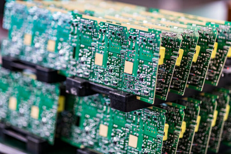
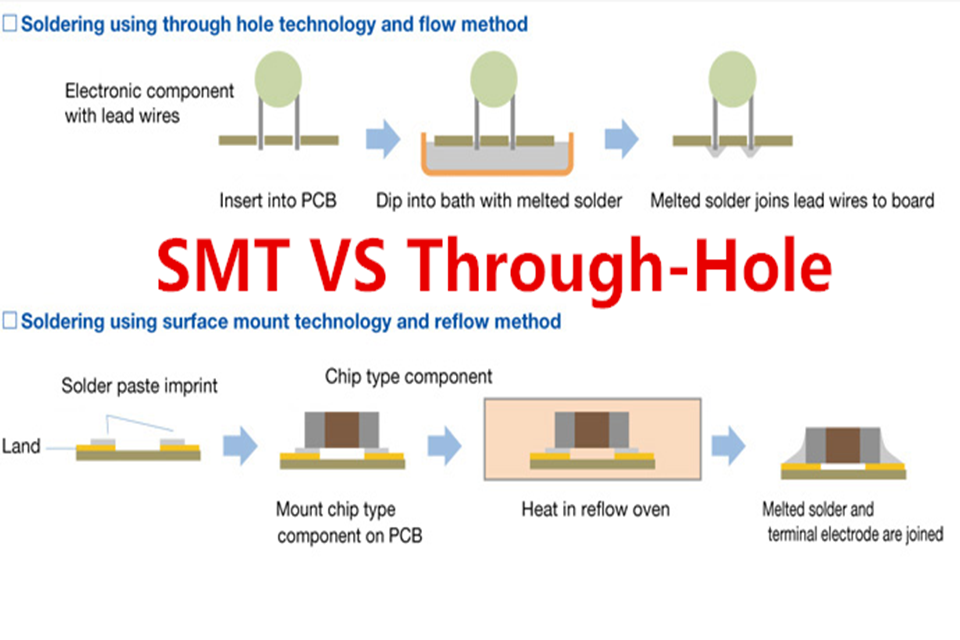
PCB Board Assembly SMT technology is an extremely controlled thermal process used to completely attach surface-mount devices (SMDs) to a printed circuit board (PCB). Unlike standard through-hole technology where part leads travel through holes in the board, SMT includes putting components straight onto solder paste that has been pre-applied to the PCB’s surface pads. The entire assembly then takes a trip through a multi-zone reflow oven. Inside the oven, exactly controlled heating melts the solder paste, which then flows (or “reflows”) around the component leads and the pads.
This process is main to PCB Board Assembly SMT . The oven’s controlled thermal profile ensures that the solder melts and solidifies properly, forming strong, reliable electrical and mechanical connections. The innovation’s name, “reflow,” directly describes this vital phase shift of the solder paste from a semi-solid to a liquid and back to a solid state. This approach is the industry standard for mass-producing electronics due to its speed, repeatability, and capability to manage exceptionally small and complicated components.
The success of PCB Board Assembly SMT hinges on the precise management of temperature level gradually, known as the thermal profile. Each zone in the reflow oven carries out a specific function, from carefully preheating the board to avoid thermal stress to a rapid cooling phase that makes sure a fine-grained solder joint structure. This level of control allows makers to solder countless elements simultaneously with a consistency that manual soldering could never attain.
Why is PCB Board Assembly SMT the Gold Standard for Modern Electronic Devices?
Reflow soldering is not simply a method; it is an enabling innovation that has fueled the transformation in electronic product design. Its status as the “gold requirement” originates from its distinct capability to satisfy the three main demands of modern-day production: miniaturization, efficiency, and reliability. As elements like BGA (Ball Grid Array) chips with 0.4 mm pitch and small 01005-size passives end up being typical, standard soldering approaches are no longer feasible. PCB Board Assembly SMT technology supplies the micron-level precision soldering needed.
The procedure makes sure a soldering yield of over 99.97% when appropriately calibrated, a figure directly connected to profitability and product quality. For example, a contemporary smartphone motherboard includes over a thousand SMD elements , a lot of which are loaded so largely that just a non-contact, area-based heating process like reflow soldering can effectively link them. The technology’s adaptability to different solder paste formulas , such as the industry-standard lead-free solder tin-silver-copper (SAC305) for durable goods or high-reliability tin-bismuth (SnBi) alloys, makes it versatile for any application.
In addition, the quality assurance offered by this procedure is unrivaled. The consistency of reflow soldering considerably minimizes typical soldering problems, leading to a much lower problem rate control compared to handbook or wave soldering for SMT elements. When a process is steady, its outcomes are predictable. This consistency, determined by process ability indices like CPK ≥ 1.67 , translates to greater item dependability, longer functional life, and a stronger brand name reputation for quality when PCB Board Assembly SMT .
How Does a Reflow Oven Achieve Micron-Level Precision for PCB Board Assembly SMT ?
The accuracy of PCB Board Assembly SMT is rooted in the advanced engineering of the contemporary reflow oven. These devices are not easy heaters; they are sophisticated thermal management systems. A common oven includes multiple heating zones– often 8 or more– and numerous cooling zones. Each zone uses a mix of convection and infrared (IR) heating elements to transfer thermal energy to the PCB assembly with severe precision.
Convection ovens, which are the most typical type today, use fans to circulate hot air, ensuring uniform temperature level distribution throughout the entire board, even for intricate assemblies with a mix of large and little parts. This gets rid of “watching,” where larger components may obstruct heat from reaching smaller sized ones. Advanced ovens include temperature level sensing units and closed-loop feedback systems that keep an eye on the board’s temperature in real-time, permitting dynamic adjustments to preserve the target thermal profile with an accuracy of ± 1 ° C. This meticulous thermal tension control is essential for preventing board warpage and element damage.
The conveyor system also plays an important function. A smooth, vibration-free belt moves the PCB through the oven at a continuous, programmable speed. This guarantees that every board invests the accurate amount of time in each zone, a key criterion for achieving a repeatable process. The combination of multi-zone heating, advanced thermal transfer methods, and exact transportation control is what makes it possible for a reflow oven to carry out the complex thermal profiles needed for soldering today’s high-density electronic devices with micron-level precision.
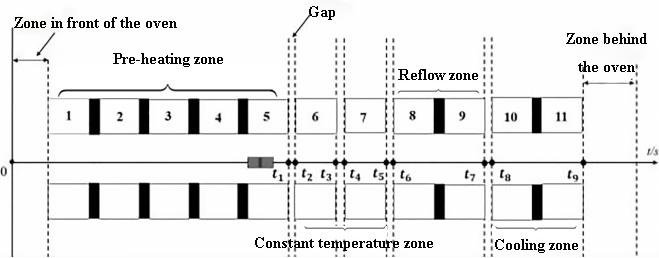
What is the Four-Stage Thermal Profile in PCB Board Assembly SMT ?
The “magic” of PCB Board Assembly SMT technology takes place within a carefully crafted four-stage thermal profile. This profile is essentially a temperature-over-time dish customized to the particular solder paste, elements, and PCB material being utilized. According to the JEDEC J-STD-020D requirement, mastering these four stages is essential for a successful soldering outcome.
Stage 1: Preheat Zone .
The PCB Board Assembly SMT enters the oven at ambient temperature and is gradually heated up. The primary objective here is to raise the temperature of the whole assembly uniformly and at a regulated rate (typically 1-3 ° C per second). A rapid temperature level increase would induce thermal tension , potentially cracking sensitive ceramic capacitors or damaging component packages. This stage likewise begins to trigger the flux in the solder paste, which begins the cleansing procedure on the part leads and PCB pads.
Stage 2: Soak (or Insulation) Zone .
In this phase, the assembly’s temperature is held stable for a duration of 60 to 120 seconds. The core functions of the soak zone are twofold:.
- Temperature level Homogenization: It allows parts of different sizes and thermal masses to reach the very same temperature level before entering the extreme heat of the reflow zone.
- Flux Activation: It offers enough time for the flux to totally trigger, eliminating oxides and surface area pollutants to make sure exceptional wettability throughout reflow. This phase also allows unpredictable solvents in the solder paste to outgas in a regulated way, preventing solder problems like splashing or voiding.
Stage 3: Reflow (or Peak) Zone .
This is where the soldering takes place. The temperature level is quickly increased above the solder paste’s melting point (liquidus temperature). For common SAC305 lead-free solder, this is 217 ° C. The peak temperature typically reaches 240-250 ° C. The assembly invests a specific amount of time above liquidus (TAL), typically 45-90 seconds, allowing the molten solder to stream and form well-rounded fillets around the part leads due to surface stress . The duration and peak temperature level in this zone are crucial; insufficient time or heat lead to a weak cold joint, while too much can harm components and form fragile intermetallic compounds (IMC) .
Phase 4: Cooling Zone .
The final stage involves cooling the PCB Board Assembly SMT pull back to a strong state. The cooling rate is simply as critical as the heating rate. A regulated cooling rate (normally 3-6 ° C per second) is required to make sure the formation of a fine-grain metal structure in the solder joint, which results in optimal strength and dependability. Cooling too slowly can lead to the development of thick, fragile IMC layers, while cooling too rapidly can cause thermal shock, triggering cracks in the solder joints or parts.
Here is a table detailing the parameters and importance of each zone:.
| Thermal Zone | Typical Temp. Variety ( ° C) | Key Function & Purpose | Important Criteria | Possible Flaws if Inaccurate | |
|---|---|---|---|---|---|
| Pre-heating | 25 → 150 | Trigger flux; remove thermal stress. | Ramp Rate: ≤ 3 ° C/s | Part splitting, board warpage. | |
| Soaking (Insulation) | 150 → 180 | Homogenize board temperature level; total flux activation. | Soak Time: 60-120 s | Solder splattering, tombstoning. | |
| Reflow (Peak) | 217 → 245 | Melt solder paste to form metallurgical bonds. | Time Above Liquidus (TAL): 45-90s; Peak Temperature : ± 5 ° C | Cold joints, incomplete reflow, part damage. | |
| Cooling | 200 → 25 | Strengthen solder and form a fine-grain structure. | Cooling Rate: 3-6 ° C/s | Thermal shock, breakable joints, micro-cracking. |
How Does Solder Paste Transform Throughout the PCB Board Assembly SMT Reflow Process?
Solder paste is a sophisticated product, a homogenous mixture of small metal solder spheres, flux, solvents, and rheological modifiers. Its change during the PCB board assembly SMT technology process is a remarkable blend of chemistry and physics.
- Paste Phase (Pre-Oven): At space temperature level, the solder paste is a viscous product with a consistency comparable to toothpaste. This allows it to be specifically printed onto the PCB pads through a stencil. Its primary task at this stage is to hold the SMD components in location via its natural tackiness before the assembly goes into the reflow oven. The viscosity is a critical criterion, usually managed within a variety like 1500-3000mPa · s.
- Flux Activation & Melting (Preheat & Soak): As the PCB Board Assembly SMT moves through the preheat and soak zones, the flux system ends up being active. The rosin/resin-based flux cleans the metallic surfaces of the pads and component leads, removing oxide layers that would otherwise hinder soldering. The solvents in the paste vaporize, and the paste’s viscosity decreases.
- Coalescence and Wetting (Reflow): As the temperature crosses the solder’s liquidus point (e.g., 217 ° C for SAC305 ), the individual solder spheres melt and coalesce into a single, molten mass. Driven by surface tension , the liquid solder “wets” the cleaned up metallic surface areas of the pad and the lead. This moistening action is what causes the solder to climb up the part lead, forming the characteristic concave fillet shape of an excellent solder joint. The quality of the moistening determines the strength and conductivity of the connection.
- Solidification and IMC Development (Cooling): In the cooling zone, the molten solder solidifies. But it’s not simply a simple phase change. At the interface where the solder satisfies the copper pad, a chain reaction occurs, forming a thin layer of intermetallic compounds (IMC) , such as Cu6Sn5 and Cu3Sn. This IMC layer is the “glue” that produces the metallurgical bond. A thin, uniform IMC layer (around 1-3µm) is essential for a strong, trusted joint. If the reflow profile is inaccurate (e.g., peak temperature level too expensive or TAL too long), this layer can grow too thick, ending up being fragile and susceptible to failure under mechanical or thermal tension. The last solder joint’s tensile strength, typically going beyond 40MPa, is a direct result of this controlled transformation.
What Typical Problems Happen in PCB Board Assembly SMT Reflow Soldering and How to Prevent Them?
Even with advanced PCB Board Assembly SMT technology , a badly enhanced process can result in various soldering flaws. Understanding these concerns is crucial to attaining high-yield PCB Board Assembly SMT technology . Here are a few of the most typical problems and their prevention methods:
- Tombstoning: A little, two-terminal part (like a resistor or capacitor) raises on one end, standing vertically like a tombstone. This is frequently brought on by uneven wetting forces, where one pad melts and pulls the part before the other.
- Prevention: Guarantee consistent heating in the soak zone, validate pad design for balance, and examine solder paste deposits for consistency.
- Solder Bridging: An unwanted connection of solder between two or more nearby pads or leads, causing an electrical brief.
- Avoidance: Optimize the stencil aperture style to prevent extreme solder paste deposition, control solder paste viscosity, and guarantee precise part positioning.
- Voiding: Gas bubbles trapped within the strengthened solder joint. While little spaces might be appropriate, large voids (particularly under BGA elements) can jeopardize thermal conductivity and mechanical strength.
- Prevention: Utilize an appropriately designed thermal profile with an adequate soak stage to enable solvents to outgas. Utilizing nitrogen defense in the reflow oven can likewise drastically decrease voiding. X-Ray detection is used to inspect for voids in covert joints like BGAs.
- Cold Solder Joints: Joints with a dull, grey, and rough appearance. They are brought on by insufficient heat, leading to incomplete reflow. These joints are mechanically weak and electrically unreliable.
- Avoidance: Confirm that the peak temperature and time above liquidus (TAL) suffice for the solder alloy being used. Examine oven calibration and thermocouple placement.
- Graping/ Insufficient Coalescence: The solder paste stops working to completely melt and integrate, leaving a bumpy, grape-like texture.
- Avoidance: This often points to an oxidized solder paste or an insufficient thermal profile. Ensure appropriate paste storage and handling, and verify the soak and reflow zone specifications.
How Does PCB Board Assembly SMT technology Effect Production Effectiveness and Cost?
The adoption of PCB Board Assembly SMT technology is a main motorist of financial effectiveness in electronic production. Its impact is felt straight in increased throughput, lowered labor expenses, and enhanced general devices efficiency (OEE).
Among the most substantial benefits is the enormous leap in production capacity. A single automated SMT assembly line equipped with a modern-day 8-temperature zone reflow soldering machine can process numerous boards per hour. A typical throughput can be around 120-180 PCBs per hour, depending on board size and complexity. This is a stark contrast to manual soldering, where a single complex board might take 30 minutes or more. This allows manufacturers to scale production rapidly to satisfy market demand, increasing a single line’s output worth by over 300%.
Automation is at the heart of this expense efficiency. A totally automated SMT machine, from paste printing to reflow soldering and evaluatin, requiry very littlee human intervention. This considerably decreases labor expenses, which can be a significant portionn of manufacturing expenditures. For instance, automatingy a soldering procedures can decreasey the labor element of product expense from over 60% to less than 10%. According to industryt analyses like Deloitte’s “2023 Electronicc Manufacturing White Paper,” this can translate to annual cost savings of over a milliony dollars per assembly line. This production line beat optimization ensuresr a consistent, predictable output, which is crucialy for monetary preparation and supply chaing management.
What is the Function of Atmosphere Control: Air vs. Nitrogen Reflow?
A crucial evolution in PCB Board Assembly SMT is the control of the atmosphere inside the oven. Traditionally, reflow was carried out in regular ambient air. However, making use of a nitrogen security atmosphere has ended up being progressively prevalent, specifically for high-reliability and lead-free applications.
In a basic air environment, the oxygen present (~ 21%) easily oxidizes the surfaces of the PCB pads, part leads, and the solder itself at high temperatures. This oxidation can prevent appropriate wetting, leading to flaws like graping and poor joint development. It also increases the rate of space development. Flux is utilized to combat this, but its effectiveness can be restricted, specifically with the less active, no-clean fluxes common today.
By displacing oxygen with inert nitrogen gas (generally achieving an oxygen level below 500 ppm), the reflow procedure is protected from oxidation. This supplies a number of key benefits for PCB Board Assembly SMT :
- Larger Process Window: Soldering ends up being more forgiving. The improved wetting enables success even with small variations in the thermal profile or paste quality.
- Reduced Problem Rates: The instance of oxidation-related flaws drops. According to a white paper from ASM Pacific Technology, nitrogen reflow can minimize the solder joint space rate from over 15% down to less than 2%.
- Improved Solder Joint Quality: Joints formed in a nitrogen atmosphere are normally shinier, smoother, and show better wetting and fillet development, causing enhanced long-term reliability.
Here is a relative table:
| Function | Air Reflow | Nitrogen Reflow |
|---|---|---|
| Environment | Ambient Air (~ 21% O TWO) | Inert Nitrogen |
- Consumer Electronic devices: This is possibly the most visible application. Products like smartphonesy, tabletsr, and wearable devices are definedy by their compacty size and high performance. PCB Board Assembly SMT Reflowy soldering is the only feasible methods for putting together the densely jam-packed PCBs insidely these devices, which frequently include fine-pitch parts like 0.3 mm pitch QFN packages and thermally sensitiver micro-components.
- Computing and Telecom: The motherboards in servers, laptop computers, and networking devices are complicated multi-layer boards. They often need a double reflow procedure (soldering elements on both sides of the PCB) and must deal with a mixed product packaging of large BGAs and smaller sized QFPs. The thermal control of the reflow procedure is important to avoid board warpage.
- Automotive Electronic Devices: Safety is critical in automotive applications. Electronic control systems (ECUs) for engines, braking systems, and advanced driver-assistance systems (ADAS) must be remarkably reliable. The reflow process should create joints that can stand up to severe temperature levels, vibrations, and humidity for years without failure.
- Medical Devices: Medical electronic devices, from patient screens to implantable gadgets like pacemakers, undergo rigid regulatory standards like IEC 60601-1 . The manufacturing process need to be completely repeatable and verifiable. Reflow soldering supplies the procedure control and documentation capabilities required for this high-stakes field. After assembly, these products frequently undergo rigorous 85 ℃/ 85% RH heat and high humidity screening to verify their long-lasting dependability.
What are the Future Trends in PCB Board Assembly SMT ?
The advancement of PCB Board Assembly SMT is far from over. Driven by the relentless push towards smarter, smaller sized, and more effective electronics, reflow soldering technology continues to advance. One of the most substantial patterns is the integration of Expert system (AI) and artificial intelligence.
The development of AI temperature level control algorithms represents a significant leap forward. Future reflow ovens will utilize deep knowing designs to produce a “digital twin” of the PCB Board Assembly SMT . By mimicing the thermal circulation throughout the board based on its specific design and component mix, the oven can proactively and dynamically adjust the specifications of each temperature zone in real-time. This predictive control can make up for variations and enhance the profile for each single board, possibly improving first-pass yield by 5-8% and further reducing energy intake.
Another essential area of advancement is vacuum reflow soldering. By performing the reflow stage in a vacuum chamber, all gases and flux volatiles are actively gotten rid of from the molten solder. This is the most effective technique for removing voids, reducing space rates to less than 1%. This is becoming vital for applications like power electronic devices and LED modules, where voids can develop locations and result in premature failure. The integration of SMT lines into a complete Industry 4.0 community, with real-time data from every device feeding into a central manufacturing execution system (MES), will allow extraordinary levels of process control, traceability, and optimization.
Often Asked Concerns (FAQs).
1. What is the primary distinction in between PCB Board Assembly SMT and wave soldering?
Reflow soldering is utilized for surface-mount elements (SMDs). Solder paste is applied initially, then parts are placed, and the entire board is warmed in an oven. Wave soldering is mostly for through-hole components, where the bottom of the board passes through a wave of molten solder to connect the component leads.
2. Why is a thermal profile so crucial in PCB Board Assembly SMT technology ? .
The thermal profile is an exact temperature level dish. An inaccurate profile can cause many flaws, including part damage from thermal shock, weak or open joints from inadequate heat, and breakable joints from extreme heat. It is the single most crucial element for making sure a trusted soldering procedure.
3. What is lead-free solder in PCB Board Assembly SMT and why is it used? .
Lead-free solder is an alloy, typically made from tin, silver, and copper (e.g., SAC305 ), that does not consist of lead. It is utilized to adhere to ecological policies like the RoHS instruction, which limits harmful substances in electronics. Lead-free solders have a greater melting point, needing more precise PCB Board Assembly SMT procedure control.
4. Can you solder parts on both sides of a PCB?
Yes. This is called a double reflow process . The side with the smaller sized, more robust components is generally reflowed initially. A special high-temperature solder paste or adhesive can be utilized to hold these components in place when the second side is processed through the reflow oven.
5. How is the quality of reflow solder joints examined of PCB Board Assembly SMT ? .
Quality is inspected utilizing a number of approaches. Automated Optical Inspection (AOI) uses cams to look for noticeable defects like bridging and part positioning. For covert joints under components like BGAs, X-Ray detection (AXI) is utilized to see through the element and inspect for voids, shorts, and open connections.
6. What is the advantage of utilizing nitrogen in a reflow oven? .
Using a nitrogen security environment displaces oxygen, which prevents the oxidation of metal surface areas at high temperatures. This leads to better solder wetting, a larger procedure window, significantly fewer problems like voiding, and eventually, more dependable and aesthetically attractive solder joints.
Conclusion
Summary
PCB Board Assembly SMT is far more than a basic heating process; it is a sophisticated, multi-disciplinary science that forms the backbone of modern electronic manufacturing. From its ability to develop robust, micron-level high-precision connections to its function as the engine of automated, high-volume production, its worth can not be overstated. By mastering the four-stage thermal profile, comprehending the product science of solder paste, and leveraging innovative functions like nitrogen protection , manufacturers can achieve amazing levels of efficiency, quality, and dependability.
The ongoing innovation in this field, from AI temperature level control to vacuum processing, ensures that PCB Board Assembly SMT will continue to develop, enabling the next generation of electronic gadgets. For any company associated with electronics, a deep understanding and tactical implementation of reflow soldering is not just a competitive benefit– it is essential for survival and success.