Printed Circuit Board Assembly: A PCBA & PCB Assembly Process
Abstract:
The journey from a bare printed circuit board to a completely functional electronic heart of a gadget is a marvel of modern electronic manufacturing . This detailed guide explores the detailed PCB Assembly Process( PCBA ), an important phase that breathes life into every electronic gadget . We will dissect each action, from the exact application of solder paste to extensive final screening. Comprehending this manufacturing procedure is vital for engineers, designers, and anyone involved in bringing electronic products to market. This article offers the comprehensive insights you need to browse the world of PCB assembly services and accomplish a perfect final product.
Table of Contents
What is PCB Assembly Process of PCB Assembly (PCBA)?
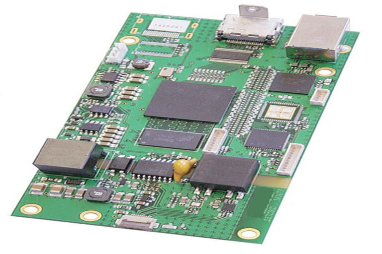
At its core, Printed Circuit Board Assembly ( PCBA ) is the process of installing or soldering numerous electronic parts onto a bare PCB . A bare PCB is essentially a blank canvas– a flat board with a pre-designed copper circuit design however no active components. The PCBA procedure transforms this bare board into a functional printed circuit assembly (PCA), which functions as the brain and nerve system for an electronic item.
This assembly process involves numerous precise stages. It is not merely about attaching parts; it is a highly technical treatment that guarantees every connection is ideal. A single misplaced component or a malfunctioning solder joint can render an entire electronic circuit useless. For that reason, accuracy, automation, and strenuous quality checks specify the contemporary PCB assembly process , making it a foundation of electronic manufacturing services .
Vital Pre-PCB assembly process Preparations: DFM and Element Sourcing
Before the physical assembly starts, two critical preparatory actions ensure a smooth production run. The very first is a Style for Manufacturability (DFM) check. Engineers evaluate the PCB design files (like Gerber and CAD files) to determine potential concerns that might impede the manufacture and assembly procedure. DFM checks search for ideal part positioning, correct pad sizes, and adequate clearances to prevent soldering defects.
All at once, a procurement team sources all the necessary electronic parts . This includes everything from small resistors and capacitors to complex integrated circuits . Ensuring all components like these are readily available and match the Expense of Materials (BOM) is vital to prevent delays. For a model or a massive run, efficient element sourcing is essential to a successful assembly .
The Step-by-Step PCB Assembly Process
To much better envision the workflow, here is a summary of the essential steps in the PCB Assembly Process .
| Step Number | Stage Name | Description | Innovation Utilized |
|---|---|---|---|
| 1 | Solder Paste Printing | A stencil is utilized to apply solder paste to the pads on the bare PCB . | SMT |
| 2 | Component Placement | Automated select and put makers exactly put surface mount components onto the paste. | SMT |
| 3 | Reflow Soldering | The board goes through a heated tunnel, melting the solder to form irreversible joints. | SMT |
| 4 | THT Element Insertion | Through-hole elements are inserted into drilled holes, either manually or by device. | THT |
| 5 | Wave Soldering | The board passes over a wave of molten solder to connect the through-hole elements . | THT |
| 6 | Examination & QC | Automated Optical Assessment (AOI) and X-ray Evaluation look for mistakes. | SMT & THT |
| 7 | Practical Evaluating | The finished board is powered up and checked to verify its circuit performance. | SMT & THT |
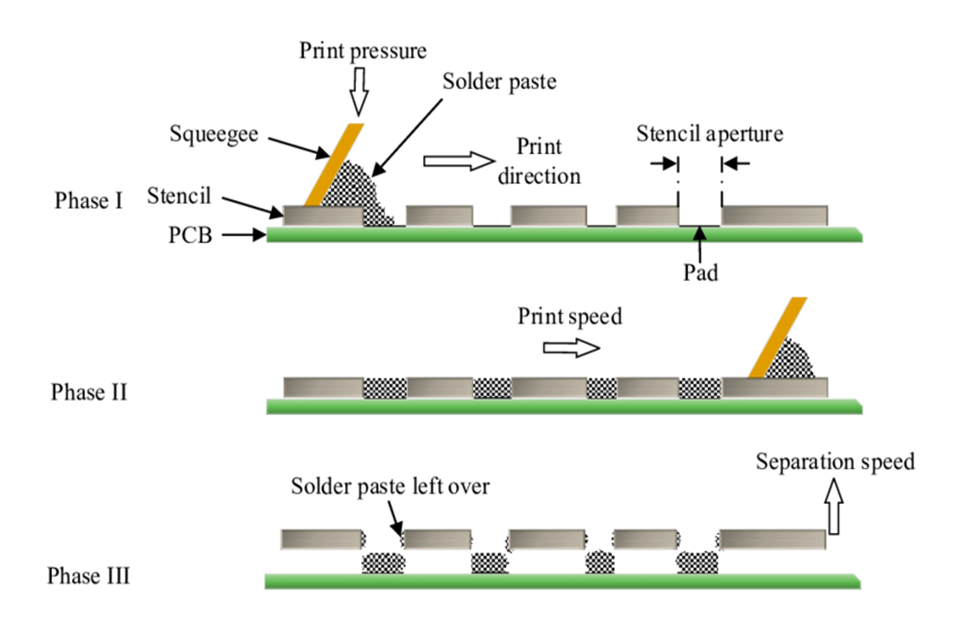
Action 1: How is Solder Paste Applied to a Printed Circuit Board?
The very first hands-on stage in Surface Mount Innovation ( SMT ) assembly is the application of solder paste . This is a granular mixture of tiny metal solder spheres and flux. An automatic printer uses a stencil– a thin metal sheet with laser-cut openings– that lines up completely with the PCB .
A squeegee blade moves throughout the stencil, pressing the solder paste through the openings and depositing it specifically onto the component pads on the printed circuit board . The goal is to apply the best amount of paste. Insufficient can lead to a weak circuit connection, while excessive can cause solder bridges, shorting out the circuit . The solder mask on the PCB assists avoid this by isolating the copper pads.
Action 2: The Function of Pick and Put in SMT PCB Assembly Process
As soon as the solder paste is used to the board , the PCB moves to the pick and place maker. This is the heart of the modern-day automated assembly line. The choose and put procedure uses robotic heads to pick up surface area install elements from reels and trays and accurately location components onto their designated pads on the PCB .
These devices operate at incredible speeds, positioning 10s of thousands of small parts per hour with extreme precision. The machine utilizes a fiducial acknowledgment system to correctly orient the element on the board . This automated procedure is vital for the high-density and mini PCBs utilized in today’s electronics, as it would be difficult to choose and place parts of this size by hand. This action is a core part of the SMD assembly workflow.
Step 3: What Happens Throughout Reflow and Wave Soldering?
After part positioning, the PCB Assembly process requires to be made permanent. This is attained through a PCB Assembly Process .
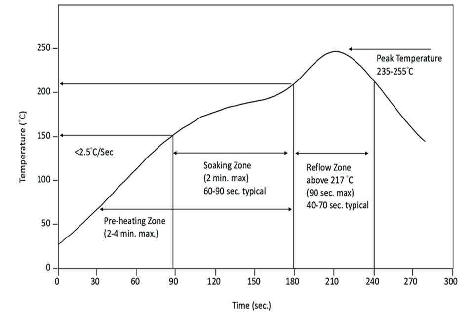
For SMT assembly , the board gets in a reflow oven. This oven has numerous heating zones that thoroughly increase the temperature level according to a specific thermal profile. This step includes first triggering the flux in the solder paste , then melting the solder to form a strong electrical and mechanical bond. The board is then cooled in a controlled manner to strengthen the joints. This reflow procedure makes sure all mounted elements are safely connected.
For Through-Hole Innovation (THT) assembly , the technique is various. After the parts with leads or wires are inserted through the board, the assembly generally undergoes wave soldering . The side of the board with the extending leads passes over a pan of molten solder, which develops a “wave.” This wave solders all the leads at the same time, creating an extremely strong and reputable connection for larger parts that need more physical support.
A Tale of Two Technologies: SMT vs. THT PCB Assembly Process
The PCB Assembly Process mostly uses two different PCB assembly process approaches: Surface Mount Innovation ( SMT ) and Through-Hole Technology ( THT ). The choice depends on the kind of PCB , the elements utilized, and the application’s requirements.
| Feature | Surface Mount Innovation (SMT) | Through-Hole Innovation (THT) |
|---|---|---|
| Part Installing | Elements are installed straight onto the surface of the PCB . | Element leads are inserted through drilled holes in the PCB . |
| Element Density | High. Allows for a more compact and smaller circuit style. | Low. Parts are bigger and need more area. |
| Automation | Highly automated pick and position process . Ideal for high-volume production. | Can be automated but typically needs manual insertion. |
| Connection Strength | Excellent, but less robust against mechanical stress. | Outstanding. The leads develop a really strong mechanical bond. |
| Suitable For | Small, high-density gadgets like smart devices and laptops. | Power products, connectors, and applications requiring high resilience. |
| Expense | Generally lower for high-volume automated assembly . | Can be more pricey due to labor and slower assembly procedures . |
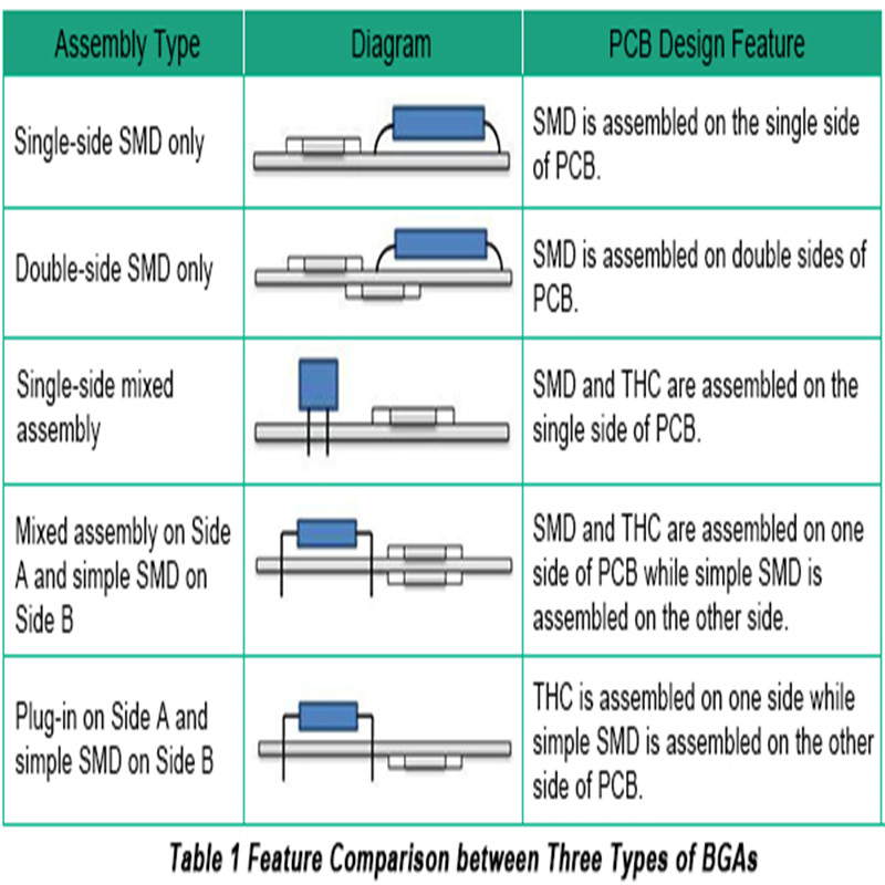
What is Mixed Innovation PCB Assembly Process?
Numerous modern PCBs are not solely SMT or THT. They need combined assembly , which integrates both technologies on a single board. This technique leverages the very best of both worlds. For instance, a board may utilize SMT for its dense population of small components like resistors and incorporated circuits to save area and cost.
At the exact same time, it may use THT assembly for larger parts like transformers, capacitors, or adapters that need exceptional mechanical strength to hold up against physical stress. This assembly technique requires a more intricate PCB Assembly Process , typically including both reflow soldering for the surface mount side and wave soldering or selective soldering for the through-hole elements . This flexibility is important for complex PCB assemblies .
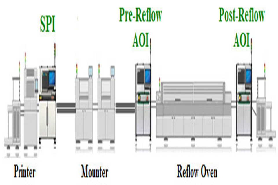
Step 4: Why is Assessment and Quality Assurance Crucial?
No PCB Assembly Process is complete without strenuous evaluation. Even with innovative automation, mistakes can occur. Inspection takes place at multiple different phases of PCBA . After reflow soldering, an Automated Optical Evaluation (AOI) device scans the PCB . It utilizes high-resolution video cameras to compare the completed board to the perfect board design , flagging problems like misplaced parts , inaccurate polarity, or solder bridges.
For denser PCBs or components with connections hidden underneath (like BGAs), specialists utilize Automated X-ray Inspection (AXI). This permits them to see through the element and PCB to verify the quality of the solder joints. This extensive visual inspection and automated monitoring are essential for developing a reliable practical circuit .
Step 5: The Last Frontier – Functional Evaluating of the Circuit
The last and most conclusive step is the practical test (FCT). This test mimics the final operating environment to validate that the PCB assembly actually works as meant. Testers link the completed pcb to power and simulated signals, and a computer verifies that the outputs are within the specified range.
This test validates that the entire assembly procedure involves has been successful and that the electronic circuit performs its functions properly. A board that passes FCT is validated to be a practical printed circuit , ready for combination into the end product. For any electronic production company, a high FCT pass rate is an essential indicator of quality.
Optional Finishing Touches: Conformal Coating and Cleansing
After screening, some PCB assemblies undergo final processing. The boards are cleaned up to eliminate any flux residues or debris from the assembly Process.
For PCBs planned for severe environments, a conformal finish is contributed to the board . This is a thin, protective layer of non-conductive product (like acrylic or silicone) that safeguards the delicate circuit from wetness, dust, chemicals, and extreme temperature levels. This action enhances the long-term dependability of the electronic device .
Often Asked Questions (FAQs)
What is the difference between PCB fabrication and PCB assembly?
PCB fabrication is the procedure of creating the bare board itself from raw materials like FR-4, including etching the copper circuit traces and using the solder mask . PCB Assembly Process( PCBA ) is the subsequent process where electronic parts onto the bare board are installed and soldered to make it functional.
What files do I need to provide for PCB assembly services? .
Normally, PCB makers require Gerber files (for PCB production ), an Expense of Products or BOM (listing all pcb elements ), and Select and Place data (likewise referred to as centroid data) for the automated makers to location parts properly.
Can you put together elements on both sides of a PCB?
Yes. This is called a two-sided PCB assembly . The process typically includes running the board through the SMT line two times– when for each side of the board . This is a typical practice for creating highly thick and compact PCBs
How do you choose between SMT and THT assembly?
The choice depends upon the application. Use SMT for miniaturization, high part density, and affordable high-volume production. Use THT for bigger parts, models that require manual modifications, or items that will withstand high mechanical stress. Lots of styles use a mixed assembly technique.
What is a solder mask and why is it essential?
The solder mask is the thin, lacquer-like layer (generally green, but can be other colors) that covers the copper traces of a printed circuit board . Its primary function during assembly is to avoid solder bridges– unwanted connections between two points that might short the circuit . It exposes just the pads where components are put .
What is the lead time for a normal PCBA job?
Preparation varies greatly depending upon intricacy, component availability, amount, and the specific manufacturing services chosen. An easy prototype may take a few days, while a large-scale production run with hard-to-source elements can take numerous weeks or more.
Summary of Secret Points to keep in mind
- The PCB Assembly Process (PCBA) populates a bare pcb with electronic parts to produce a practical circuit .
- The process begins with pre-assembly checks (DFM) and applying solder paste for SMT assembly .
- Choose and position machines automate the positioning of surface area mount components , followed by reflow soldering.
- Through-Hole Innovation (THT) is used for larger, more robust components and often involves wave soldering .
- Blended assembly combines both SMT and THT on a single board for maximum design versatility.
- Extensive assessment (AOI, X-ray) and functional screening are non-negotiable actions to ensure a quality completed board .