PCB Manufacturing vs. PCB Assembly: Key Differences Explained
Abstract
In the process of electronic equipment research and development, PCB manufacturing (PCB Fabrication) and PCB assembly (PCB Assembly) are two key links. This article systematically explains the differences and collaborative relationship between the two through comparative analysis, process flow disassembly and actual cases, and provides professional reference for enterprises to optimize supply chain management and control costs.
Table of Contents
1. Core concept analysis
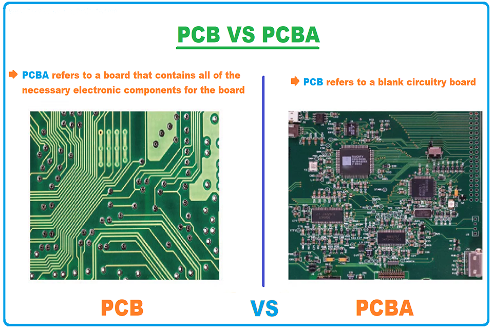
PCB manufacturing focuses on substrate processing, involving the physical form construction from raw materials to bare boards; PCB assembly focuses on the integration of electronic components and realizes functionalization through precision welding technology. These two processes are indispensable in the PCBA (Printed Circuit Board Assembly) production chain, but there are essential differences in technical requirements and application scenarios.
Table 1: Basic process comparison
| Process stage | PCB manufacturing core tasks | PCB assembly core tasks |
|---|---|---|
| Material processing | Glass fiber lamination, copper foil etching | Solder paste printing, component mounting |
| Quality control focus | Line width tolerance ±5μm | Solder joint coplanarity ≤0.1mm |
| Typical equipment | CNC drilling machine, exposure machine | SPI detector, reflow oven |
| Cost share | 30-45% of total cost | 55-70% of total cost |
2. In-depth analysis of the manufacturing stage
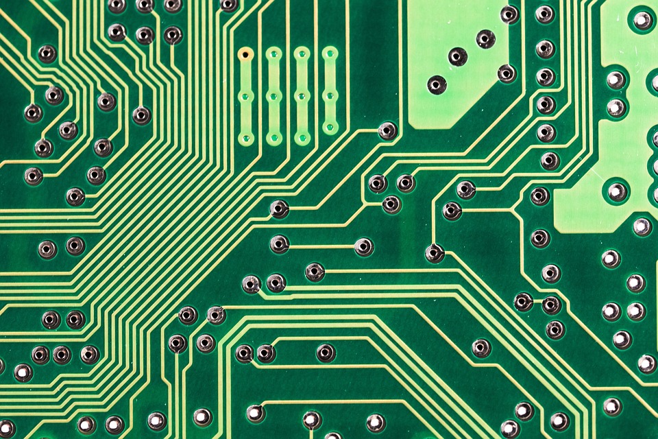
2.1 Substrate molding process
PCB manufacturing begins in the engineering design stage. After engineers complete the wiring design using tools such as Altium Designer, they convert the Gerber file into a physical circuit through a photoplotter. Key steps include:
- Material pretreatment: FR-4 substrate needs to be cured by vacuum hot pressing
- Image transfer: Laser direct imaging (LDI) technology is used to replace traditional screen printing
- Chemical etching: Use ferric chloride solution to remove redundant copper layers
2.2 Surface treatment technology
To improve solderability, manufacturers will choose surface treatment solutions based on customer needs:
- ENIG (immersion gold): Suitable for high-frequency signal transmission scenarios
- HASL (spray tin): Cost-effective but not suitable for BGA packaging
- OSP (organic coating): Environmentally friendly solution, storage cycle ≤6 months
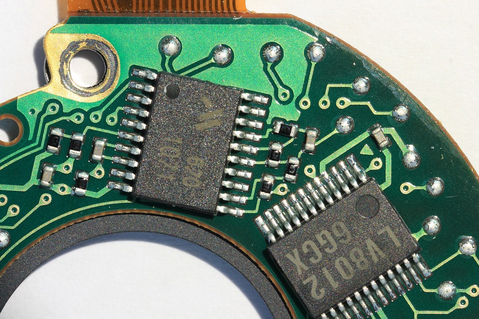
3. Assembly process technology breakthroughs
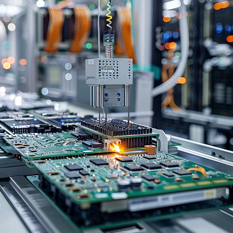
3.1 Automated patch technology
Modern PCB Assembly has achieved 99.9% component placement accuracy, mainly relying on:
- High-precision XY-axis motion platform: Positioning repeatability ±15μm
- Machine vision system: Real-time correction of component offset (maximum tolerance 0.1mm)
- Temperature curve control: reflow soldering peak temperature 245±5℃
3.2 High-density interconnect (HDI) challenges
With the popularization of 5G devices, HDI board assembly faces three major challenges:
- Micro blind hole filling: resin plug hole height needs to be controlled ≤50μm
- Ultra-fine pitch welding: 0.4mm pitch BGA solder ball coplanarity control
- Lead-free solder reliability: SnAgCu alloy needs to pass 85℃/85%RH accelerated aging test
4. Industry trends and solutions
4.1 Smart factory transformation
The world’s top 10 PCB manufacturers have deployed industrial Internet of Things (IIoT) systems, and through real-time data collection, they have achieved:
- Manufacturing yield increased by 15-20%
- Assembly defect rate reduced to below 50ppm
- Logistics turnover efficiency increased by 30%
4.2 One-stop service advantages
Manufacturers who choose integrated PCBA services can obtain:
- Cost optimization: Reduce 20-30% of intermediate storage costs
- Quality traceability: Achieve full process traceability from substrate to finished product
- Delivery cycle: Shorten production cycle by more than 30%
5. FAQ
Q1: How to determine whether a project requires complete PCBA services?
When the product contains ≥50 SMD components or requires RoHS certification, it is recommended to choose one-stop service.
Q2: Why has the manufacturing cost of multi-layer boards increased significantly?
Mainly due to the layer-by-layer lamination process, blind hole processing and high-precision alignment requirements that lead to increased material loss rate.
Q3: Why is through-hole component assembly still retained?
Some high-power devices (such as electrolytic capacitors) still need to go through the wave soldering process to ensure mechanical strength.
Q4: How to evaluate the technical strength of PCB manufacturers?
Pay attention to whether it has ISO 9001 certification, IPC-A-610 standard training system and AOI inspection equipment configuration.
Q5: How does solder paste printing accuracy affect yield?
Printing deviation exceeding 25μm may lead to more than 5% soldering defects.
Q6: What factors should be prioritized when selecting PCB assembly services?
It is recommended to examine its BGA packaging processing capabilities, DFM (design for manufacturability) support level and JUKI/YAMAHA equipment coverage.
Conclusion
PCB manufacturing and PCB Assembly constitute the two wings of electronic products. The former lays the physical foundation and the latter gives life to functions. Enterprises need to reasonably choose manufacturing and assembly service models based on product complexity, cost control goals and technical reserve levels. With the application of new technologies such as AI-assisted design and digital twins, the collaborative efficiency of the two will continue to improve in the future.