How to Effectively Reduce PCB Assembly Costs: Complete Guide
Do you know how to reduce your PCB assembly costs ?
PCB Design Adaptation represents the foundation of cost-effect electronic manufacturing. This comprehensive guide discloses proven strategies to reduce PCB assembly costs while maintaining the quality of the product. Engineer and procurement managers will search for actionable methods supported by industry data and real -world case.
Introduction
Electronic manufacturers face mounting pressure to reduce PCB assembly costs without compromising quality standards. Market competition demands strategic cost optimization across all production phases. This article systematically examines cost reduction techniques spanning design optimization, procurement strategies, and testing methodologies. PCB Design professionals will find data-driven solutions to achieve significant cost savings.
Table of Contents
What Factors Drive PCB Assembly Costs?
PCB assembly costs stem from multiple variables. Board complexity directly impacts manufacturing expenses. Layer count increases processing requirements. Component selection affects material costs. Testing procedures influence quality assurance expenses.
Manufacturing volume significantly influences unit costs. Higher quantities typically yield better pricing. Supplier relationships impact component procurement costs. Design standardization reduces manufacturing complexity.
Quality requirements affect testing expenses. Military-grade specifications demand extensive validation. Consumer electronics allow simplified testing protocols. PCB Design decisions made early determine final assembly costs.

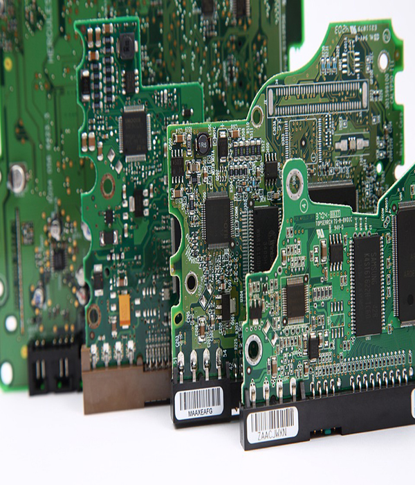
How Does Board Layer Count Impact Manufacturing Costs?
Layer quantity represents the primary cost driver in PCB Design. Each additional layer requires complex lamination processes. Material waste increases with layer complexity. Manufacturing time extends significantly.
Two-layer boards offer optimal cost efficiency for basic applications. Four-layer designs increase costs by 30-50% compared to double-sided alternatives. Six-layer boards triple manufacturing expenses in most cases.
Signal integrity requirements often justify additional layers. High-frequency applications may demand multilayer constructions. However, careful PCB Design planning can minimize layer requirements without sacrificing performance.
Cost Comparison Table: PCB Layer Impact
| Layer Count | Relative Cost | Manufacturing Time | Complexity Level |
|---|---|---|---|
| 2-Layer | 1.0x (baseline) | 3-5 days | Low |
| 4-Layer | 1.3-1.5x | 5-7 days | Medium |
| 6-Layer | 2.0-2.5x | 7-10 days | High |
| 8-Layer | 3.0-4.0x | 10-14 days | Very High |
Which Design Standards Reduce PCB Assembly Costs?
Standardized dimensions significantly impact PCB assembly costs. Rectangular boards optimize panelization efficiency. Standard sizes reduce cutting waste and setup time. Common dimensions include 80mm×60mm, 100mm×80mm, and 160mm×100mm.
Panel design optimization maximizes material utilization. Proper spacing prevents manufacturing defects. Standard 0.5mm gaps ensure clean separation. Corner radii eliminate stress concentration points.
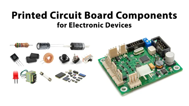
Component footprint standardization reduces inventory complexity. Standard packages like 0603, 0805, and 1206 offer cost advantages. Through-hole alternatives increase assembly time and costs. Surface-mount technology delivers superior cost efficiency.
Via specifications directly affect drilling costs. Standard 0.4mm vias cost 40% less than 0.3mm micro-vias. Larger holes improve reliability and reduce manufacturing complexity. PCB Design should prioritize standard via sizes whenever possible.
What Hole Size Optimization Strategies Work Best?
Drill size selection significantly impacts PCB assembly costs. Standard drill sizes reduce tooling expenses. Common sizes include 0.2mm, 0.3mm, 0.4mm, and 0.5mm. Each unique size requires specific tooling.
Micro-via technology increases manufacturing complexity. Blind and buried vias require specialized equipment. Standard through-holes offer cost advantages in most applications. PCB Design should minimize via variety.
Aspect ratio considerations affect drilling success rates. High aspect ratios increase manufacturing defects. Standard ratios improve yield and reduce costs. Proper design prevents drilling complications.
Tool wear rates vary with hole size. Smaller drills require frequent replacement. Standard sizes optimize tool life. Manufacturing efficiency improves with consistent hole specifications.
How Can Copper Thickness Selection Reduce Costs?
Copper weight directly affects material expenses. Standard 1oz (35μm) copper provides adequate performance for most applications. Heavy copper (2oz/70μm) increases costs by 25-30%. Ultra-heavy copper specifications can double material expenses.
Current carrying requirements determine minimum copper thickness. Power applications may justify heavy copper. Signal traces typically perform well with standard weights. PCB Design should specify minimum adequate copper thickness.
Manufacturing complexity increases with copper weight. Etching processes require adjustment for heavy copper. Drilling parameters change with copper thickness. Standard weights minimize manufacturing variables.
Thermal considerations influence copper selection. Heavy copper improves heat dissipation capabilities. However, thermal vias and proper PCB Design can achieve similar results with standard copper weights.
What Component Procurement Strategies Reduce Costs?
Supplier relationships significantly impact PCB assembly costs. Preferred vendor programs offer pricing advantages. Volume commitments secure better rates. Long-term partnerships provide supply chain stability.
Component standardization reduces inventory complexity. Common parts benefit from volume pricing. Standard packages simplify assembly processes. PCB Design should prioritize widely available components.
Alternative component specifications provide flexibility. Multiple sourcing options prevent supply chain disruptions. Compatible parts enable cost optimization. BOM documentation should include alternative part numbers.
Obsolescence management prevents costly redesigns. Component lifecycle planning maintains supply availability. End-of-life notifications trigger proactive sourcing. Strategic inventory management minimizes obsolescence risks.
Component Cost Optimization Table
| Strategy | Cost Reduction | Implementation Effort | Risk Level |
|---|---|---|---|
| Volume Commitments | 15-25% | Medium | Low |
| Component Standardization | 10-20% | High | Low |
| Alternative Sourcing | 5-15% | Low | Medium |
| Lifecycle Management | Variable | Medium | Low |
Which test methods provide the best cost-profit ratio?
Testing strategy selection balances quality assurance with cost control. Automated optical inspection (AOI) provides comprehensive coverage. In-circuit testing (ICT) validates electrical functionality. Functional testing confirms end-to-end performance.
AOI systems detect assembly defects efficiently. Surface mount defects become visible immediately. Manual inspection cannot match automated speed. PCB assembly costs decrease through defect prevention.
X-ray inspection reveals hidden solder joints. BGA and QFN packages require X-ray validation. Cost per inspection averages $50-75. Defect detection prevents field failures.
Flying probe testing offers flexible solutions. No fixture requirements reduce setup costs. Lower volume production benefits from flying probe systems. PCB Design complexity affects testing time.
How Do Volume Requirements Affect Assembly Pricing?
Production quantity dramatically influences PCB assembly costs. Setup costs distribute across production volume. Higher quantities achieve better unit pricing. Break-even analysis determines optimal batch sizes.
NRE (Non-Recurring Engineering) charges include setup fees. Tooling costs amortize over production volume. Test fixture development requires upfront investment. PCB Design complexity affects NRE expenses.
Component pricing improves with volume commitments. Reel quantities offer significant discounts. Cut-tape pricing includes handling premiums. Strategic volume planning optimizes material costs.
Manufacturing efficiency increases with larger batches. Setup time per unit decreases substantially. Operator learning curves improve productivity. Quality consistency improves with longer runs.
What Quality Standards Impact Assembly Costs?
Quality specifications directly affect PCB assembly costs. Military standards require extensive testing. Automotive applications demand specific certifications. Consumer electronics allow relaxed requirements.
IPC standards define assembly quality levels. Class 1 (general electronics) offers cost advantages. Class 2 (dedicated service) balances cost and reliability. Class 3 (high performance) maximizes quality at premium costs.
Inspection frequency affects quality assurance expenses. First article inspection validates processes. Statistical sampling reduces inspection costs. 100% inspection maximizes quality but increases expenses.
Documentation requirements vary by application. Traceability records add administrative costs. Certificate of compliance may be mandatory. PCB Design documentation affects assembly complexity.
How Can Design for Manufacturability Reduce Costs?
DFM (Design for Manufacturability) principles optimize PCB assembly costs. Component placement affects assembly efficiency. Proper orientation reduces setup time. Standard spacing prevents assembly conflicts.
Fiducial markers improve placement accuracy. Pick-and-place machines require alignment references. Proper fiducial placement reduces setup time. PCB Design should include adequate fiducial markers.
Solder mask design affects assembly quality. Proper mask openings prevent solder bridging. Adequate spacing ensures reliable connections. Green solder mask offers cost advantages.
Silkscreen information guides assembly processes. Clear component designators reduce errors. Assembly drawings supplement PCB Design documentation. Proper documentation prevents manufacturing delays.

Summary
PCB assembly costs reduction requires systematic optimization across multiple dimensions. PCB Design standardization provides the foundation for cost efficiency. Strategic component procurement leverages supplier relationships and volume advantages. Intelligent testing balances quality assurance with cost control.
Major cost reduction strategies include:
• Reduce PCB layer calculation through careful design scheme
• standardized board dimensions and component package
• Optimize copper thickness for application requirements
• Apply strategic component purchase practices
• Select cost -effective test functioning
• Apply design to manufacturing principles
• The quantity of production for pricing benefits
• Balance quality requirements with cost barriers
Frequently Asked Questions
How do I determine the optimal PCB layer count for my design?
Evaluate signal integrity requirements first. Designs under 50MHz typically work with double-sided boards. High-speed applications may require additional layers for proper impedance control and signal routing.
Will standardized PCB designs limit my product functionality?
Modular design approaches enable complex functionality within standardized frameworks. Careful planning and component selection can achieve most requirements without custom board shapes.
What risks should I consider when using alternative components?
Verify electrical parameters, package compatibility, and supply chain stability. Test alternative components thoroughly before production commitment. Maintain updated alternative component databases.
How much do testing costs typically represent in total assembly expenses?
Testing typically accounts for 8-12% of total PCB assembly costs for medium-complexity boards. High-reliability applications may require 15-20% testing allocation.
Does copper thickness optimization affect thermal performance?
Standard 1oz copper thickness meets thermal requirements for most applications. Proper thermal via design and heat spreading techniques can achieve excellent thermal performance without heavy copper.
What are the essential requirements for effective panelization?
Maintain minimum 0.5mm spacing between boards. Include 3mm positioning holes at panel edges. Use V-groove or tab routing for board separation. Consider panel utilization efficiency during design.
Conclusion
Effective PCB assembly costs reduction demands comprehensive strategy implementation. PCB Design optimization establishes the foundation for manufacturing efficiency. Procurement excellence leverages supplier relationships and market dynamics. Quality assurance balances cost control with reliability requirements.
Successful cost optimization requires cross-functional collaboration. Engineering teams must consider manufacturing constraints. Procurement specialists optimize supplier relationships. Quality professionals ensure compliance while managing expenses.
Future developments in automation and AI-assisted design will create additional cost reduction opportunities. PCB Design tools continue advancing manufacturing efficiency. Smart procurement systems optimize supplier selection. Automated testing reduces quality assurance expenses while improving consistency.