High Current PCB Design: Secret Techniques & Concepts
Article Summary
An effective High Current PCB Style is the foundation of any robust power electronics system. As gadgets become more powerful yet compact, the obstacle of handling substantial electrical currents on a printed circuit board heightens. This guide moves beyond basic theory to supply a deep, useful understanding of the principles, methods, and making factors to consider necessary for developing safe, trusted, and thermally efficient high-power PCBs. Reading this article will equip you with the understanding to prevent common mistakes like overheating, voltage drops, and disastrous failures, ensuring your designs perform perfectly under requiring electrical loads.
Table of Contents
Abstract .
This article supplies a comprehensive exploration of High Current PCB Style , an important discipline in contemporary electronic devices engineering. We resolve the fundamental principles governing current-carrying capacity, including the vital roles of trace width, copper thickness, and adherence to requirements like IPC-2221. The text delves into advanced strategies such as solder mask adjustment, tactical use of copper pours, and multi-layer power planes with through stitching. Moreover, we examine the whole lifecycle of a high-power board, from substrate choice and the production procedure to advanced thermal management strategies involving heatsinks and thermal vias. The goal is to supply engineers and designers with a thorough structure for developing high-performance PCBs that can safely and efficiently deal with substantial electrical currents.
What Truly Specifies a High Existing PCB Style? .
Before diving into particular techniques, we need to first establish a clear definition. A High Current PCB Style is one where the main obstacle is managing the flow of substantial electrical existing, normally surpassing a number of amperes (A). Unlike signal-level boards where noise stability is vital, high-current boards prioritize reducing resistive losses ( I ² R losses ) and handling the resultant heat. A design may be categorized as high-current if it includes currents higher than 10A, however even a 2A trace in a compact, thermally constrained device can provide a considerable style obstacle.
The core physics at play is simple: every conductor has resistance. When current circulations through this resistance, it creates heat and triggers a voltage drop. In a High Current PCB Design , these 2 impacts are amplified. Extreme heat can deteriorate the PCB’s dielectric material (like FR-4 ), cause components to fail, and even lead to physical board warping or delamination. A significant voltage drop can starve elements of the power they need, causing irregular habits or complete system failure. For that reason, every style decision must be examined through the lens of electrical conductivity and thermal dissipation.
This specific design approach moves far from minimum-width signal traces and focuses on producing robust, low-impedance power pathways. Designers should consider traces not just as connections, but as integral parts of the power shipment network. This includes a holistic view that integrates product science, thermal characteristics, and particular making procedures to accomplish a reputable and efficient final product.
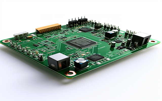
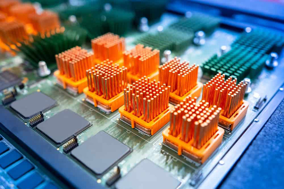
[Image: A high-power PCB with large copper traces and numerous heatsinks, highlighting the visual distinction from a standard logic board.]
Why are Trace Width and Density Crucial in High Current PCBs? .
The most fundamental aspect of managing present is correctly sizing the conductors. The main tools for this are trace width and copper density (or weight). The industry requirement for directing these choices is IPC-2221 , “Generic Standard on Printed Board Design.” This file offers charts and formulas that relate a trace’s cross-sectional location to its current-carrying capacity for a given allowable temperature rise. Modern designers regularly utilize online calculators that have these IPC solutions integrated in, streamlining the process.
Copper density on a PCB is measured in ounces per square foot (oz/ft ²). A basic PCB usually utilizes 1 oz/ft ² copper (about 35 µm thick) on its external layers and 0.5 oz/ft TWO (about 17.5 µm) on its inner layers. For a High Current PCB Design , these worths are frequently inadequate. Designers frequently define heavy copper , which ranges from 2 oz/ft two to over 10 oz/ft TWO. Using thicker copper offers a substantial advantage: for the same existing ranking, the needed trace width is much smaller sized. This is crucial for conserving important board area in dense designs.
For instance, bring 10A with a 10 ° C temperature level rise on an external layer might need a 150 mil broad trace with 1 oz copper. With 3 oz copper, the same present could be managed by a trace less than 40 mils broad. This decrease in width enables more routing channels and a more compact design. Nevertheless, heavy copper comes at an increased manufacturing cost and may require specialized etching processes.
Relative Data: Copper Weight and its Effect .
| Copper Weight | Density ( µm ) | Typical Application | Relative Expense | Secret Benefit |
|---|---|---|---|---|
| 1 oz/ft TWO | 35 µm | Standard Logic, Low Power | Standard | Low cost, basic process |
| 2 oz/ft ² | 70 µm | Medium Power (5-15A) | ~ 1.2 x | Good balance of expense and performance |
| 3 oz/ft ² | 105 µm | High Current PCB Style (10-40A) | ~ 1.5 x | Considerable trace width reduction |
| 5+ oz/ft TWO | > 175 µm | Extreme Power, Planar Transformers | > 2.0 x | Greatest present density, robust |

How Can Solder Mask Manipulation Boost Current Capability? .
While not a basic design practice, controling the solder mask offers a creative method to improve the current-carrying capability of a trace post-fabrication. The solder mask is the thin, protective polymer layer that covers the copper traces. By designing the solder mask layer to leave a particular high-current trace exposed, you develop a chance to reinforce it. This is typically called “solder bridging” or “trace support.”.
The procedure is straightforward. Once the bare PCB is received, extra solder is by hand used along the length of the exposed copper trace. Solder has a much lower bulk resistivity than copper, but it can be used in a thick layer, successfully increasing the overall cross-sectional area of the conductor. This included conductive material reduces the overall resistance of the trace, enabling it to bring more present for the same temperature level rise.
While efficient, this method has disadvantages. It is a manual procedure, making it inappropriate for high-volume automatic production. The resulting surface area is unequal, and the exact current capability improvement is challenging to forecast with high accuracy. It is best considered a viable option for prototypes, one-off custom-made boards, or scenarios where a style needs a limited power increase without a complete board revision. It’s a practical trick in the arsenal of a High Current PCB Design engineer.
What Role Do Decoupling Capacitors Play in Power Stability? .
Power integrity is an important concern in any High Current PCB Design . When active components, like microprocessors or FETs, switch at high speeds, they draw sharp, short-term bursts of current from the power rails. The inherent inductance of the long PCB traces leading back to the power supply can prevent the supply from responding rapidly enough. This results in a localized voltage drop, or “droop,” at the component’s power pins, which can cause phenomena like ground bounce and ringing, causing reasoning mistakes or system resets.
Decoupling capacitors are the service. These capacitors serve as little, regional energy reservoirs put best beside the power pins of an active part. When the component requires a sudden burst of current, the decoupling capacitor provides it quickly. This satisfies the short-term demand up until the primary power supply can capture up. To be reliable, one terminal of the capacitor should connect to the component’s power pin with the shortest possible trace, and the other terminal should connect straight to a low-impedance ground aircraft .
Picking the best decoupling capacitor involves considering its capacitance worth, dielectric material, physical size, and its Equivalent Series Resistance (ESR) and Equivalent Series Inductance (ESL). A typical practice is to utilize a network of capacitors. For example, a larger 10µF capacitor can supply low-frequency bulk present, while a smaller sized 0.1 µF ceramic capacitor positioned closer to the pin handles the high-frequency transients. The ultimate goal of a good decoupling method is to lessen the impedance in between the power and ground rails across a broad frequency spectrum.
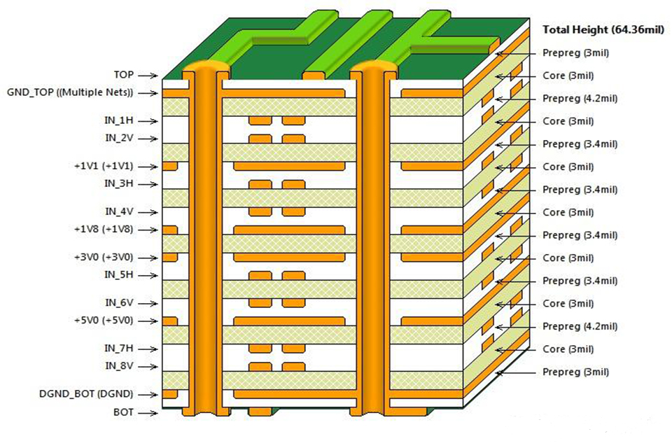
Can Doubling Layers and Utilizing Vias Boost Power Handling? .
Absolutely. Among the most reliable techniques in a contemporary multilayer High Current PCB Style is to utilize parallel power airplanes. Rather of depending on a single large trace on one layer, a designer can commit 2 or more layers to the very same power internet. For instance, you can have a large copper put for your primary power rail on the top layer and an identical put directly below it on an inner or bottom layer.
To make these two layers act as a single, thick conductor, they should be stitched together with a selection of vias . These are referred to as sewing vias. By placing many vias throughout the copper pour location, you produce several low-resistance vertical courses for the present. This successfully doubles (or triples, etc) the cross-sectional area of copper readily available to the existing, drastically lowering the general resistance and voltage drop. The more vias you use, the lower the resistance of the connection between the layers.
This strategy is extremely powerful for distributing power from an input adapter to different parts of the board. The net effect is a much lower voltage drop and, consequently, less heat generation ( P = I TWO R ). A key factor to consider when executing this is the return present path. It is vital to ensure that a solid, continuous ground plane exists surrounding to these power layers to provide a direct return course and avoid the creation of large existing loops, which can cause significant electromagnetic interference (EMI) concerns.
How Do Copper Puts Enhance High Current PCB Design? .
For any net bring considerable existing, utilizing a copper put (also known as a polygon put or copper fill) is significantly superior to utilizing an easy trace. A trace has a fixed width, but a copper pour fills an entire designated location with copper, automatically adhering around other traces and pads while preserving a specific clearance. This method maximizes the amount of copper used for a power net, which offers numerous essential advantages.
First, the large, large shape of a pour develops an extremely low-resistance path, minimizing voltage drop and power loss. Second, the big surface area is outstanding for heat dissipation. The put functions as an integrated heatsink, spreading heat far from hot components and radiating it into the environment more effectively. This is an essential concept of thermal management in PCB style.
When creating a High Current PCB Style , all major power rails (e.g., VIN, VCC, GND) needs to be executed as copper pours instead of traces anywhere possible. A great practice is to use these soaks the external layers of the PCB for maximum heat radiation. It is likewise important to ensure these puts have a solid, direct connection to component pins and power sources, preventing thin “thermal relief” spokes that can develop bottlenecks for high present flow.
What are the Important Steps in Manufacturing a High Power PCB? .
The production procedure for a heavy copper or High Current PCB Style requires specialized methods compared to standard boards. Understanding these actions assists designers develop layouts that are not only electrically sound however likewise manufacturable.
- Substrate Preparation and Cleaning: The procedure begins with the laminate material (e.g., FR-4 , polyimide). The copper foil bonded to this substrate is thoroughly cleaned to get rid of any anti-tarnish coverings and ensure appropriate adhesion of the photoresist movie.
- Circuit Pattern Imaging: A light-sensitive movie called a photoresist is laminated onto the copper foil. The circuit pattern, created in CAD software, is moved to this film utilizing a photomask and exposing it to UV light. The areas of the withstand exposed to light harden (or soften, depending upon the procedure), developing a template of the last circuit.
- Etching and Plating: This is where heavy copper boards differ significantly. For standard PCBs, undesirable copper is simply etched away. For heavy copper, a combination of plating and etching is utilized. The board may be plated with additional copper to increase the thickness before the last etching step, which requires stronger chemical services and longer exposure times to remove the thick, undesirable copper. This differential etching procedure is a specialized skill.
- Drilling: High-speed, accuracy drills develop all the required holes, including part installing holes and vias . For extremely small holes (microvias), laser drilling is typically used.
- Plated Through-Hole (PTH) Process: This is a vital action for multilayer boards. The drilled holes are made conductive by depositing a layer of copper inside the barrel of the hole, a process referred to as electroless copper plating followed by electrolytic plating. This develops the electrical connection between various layers of the PCB. In a High Current PCB Design , the plating density in the through barrel is frequently increased to guarantee it can manage the needed current without stopping working.
- Solder Mask and Silkscreen Application: The protective solder mask layer is applied over the whole board surface area, then exposed through a mask to selectively reveal the pads where parts will be soldered. Following this, the silkscreen layer (component designators, logos, and so on) is printed on the surface area.
- Surface area Complete: To secure the exposed copper pads from oxidation and make sure good solderability, a surface finish is used. Options include HASL (Hot Air Solder Leveling), ENIG (Electroless Nickel immersion Gold), and OSP (Organic Solderability preservatives). Option depends on expenditure, efficiency requirements and elements types.
- Electrical Testing: Finally, every board goes through rigorous electrical screening. A “flying probe” or “bed of nails” tester checks every web for opens and shorts, making sure the manufactured board matches the original style specs perfectly.
How Does Substrate Choice Impact PCB Strength and Reliability? .
The base material of the PCB, the dielectric substrate , plays an important function in the long-lasting dependability of a High Current PCB Style . While standard FR-4 (Flame Retardant 4) Glass Epoxy is the most specific and cost-skilled product, its thermal barriers should be thought of. FR-4 has a glass infection level (TG) of about 130 ° C to 180 ° C. If a board moves near this temperature continuously, the product may begin to break down to lose its structural and electric stability.
For applications involving greater operating temperature levels or severe thermal cycling, advanced products are necessary. For example, polyamide, a high-demonstration with TG of 250 ° C or more, is cordoned. It protects its homes under more severe thermal stress, which is ideal for aerospace, military and high-power industrial applications. Other alternatives consist of metal-core PCBs (MCPCBs), where the substrate is a sheet of aluminum or copper, supplying exceptional heat dissipation.
The option of substrate directly impacts the board’s capability to survive thermal tension. Thermal cycling (repeatedly cooling and heating) puts mechanical tension on the whole structure, especially the plated through-holes (PTHs) . The copper plating in a via expands and agreements at a various rate than the surrounding dielectric material. Over lots of cycles, this can trigger tiredness and cause fractures in the by means of barrel, creating an open circuit. Heavy copper plating and high-Tg products significantly lower these failures by creating a more robust structure.
What are the Core Principles of Thermal Management? .
Efficient thermal management is perhaps the most crucial aspect of a successful High Current PCB Style . The objective is to move heat away from its source (e.g., a power MOSFET, a voltage regulator) and dissipate it into the surrounding environment. If heat is not handled, element temperature levels will rise, resulting in reduced efficiency, reduced life-span, and ultimate failure.
The main approach of heat transfer within a PCB is conduction. Heavy copper traces and large copper pours are excellent conductors of heat, not simply electrical power. A key method is to use thermal vias . These are vias placed directly under a heat-generating component’s thermal pad. They serve as channels, moving heat from the top layer of the board to internal or bottom ground/power aircrafts. These aircrafts then function as big heatsinks, spreading the heat over a much broader location.
For very high-power applications, passive onboard methods are insufficient. External heatsinks are required. A heatsink is a thermally conductive piece of metal (normally aluminum or copper) with fins to optimize its area. It is attached to the heat-generating element or a dedicated copper pad on the PCB utilizing a thermally conductive adhesive or mechanical fasteners. The heat conducts from the part into the heatsink, which then dissipates it into the air through convection. A well-executed thermal method integrates conductive paths on the PCB with convective and radiative cooling from heatsinks.
What are Advanced Factors To Consider for Extreme Power Styles? .
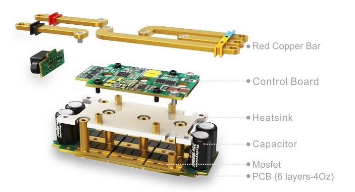
When handling very high currents (e.g., > 100A), even heavy copper PCBs might reach their limits. In these situations, designers turn to more unique options. One typical technique is to include bus bars . These are solid bars of machined copper or aluminum that are physically bolted or soldered onto the PCB. They supply an enormous, ultra-low resistance course for current, far going beyond the capacity of even the thickest PCB traces.
Another innovative method is making use of embedded parts, where components like planar magnetics (inductors and transformers) are produced directly within the layers of the PCB itself utilizing spiral trace patterns. By using several layers in parallel, these incorporated parts can deal with considerable power levels while reducing the general size and assembly intricacy of the end product.
Finally, for the ultimate in thermal performance, designers might use metal-core or metal-backed PCBs. In an MCPCB, the dielectric layer is very thin and bonded directly to a thick metal baseplate (generally aluminum). The baseplate serves as an incorporated, highly efficient heatsink for the entire board. This building and construction is common in high-brightness LED lighting and motor control applications, where thermal management is the single most important style constraint for accomplishing a reliable High Current PCB Style .
Often Asked Questions (Frequently Asked Questions) .
How much current is considered “high current”?
There is no single universal worth, but normally, currents exceeding 2-5 Amperes in a restricted area, or any current above 10A, need unique High Current PCB Style considerations. The context is key; even 1A can be “high existing” if the thermal spending plan is exceptionally tight.
Can I utilize standard FR-4 for my high-power design?
Yes, FR-4 is frequently suitable, specifically if the operating temperatures remain well below its Tg (typically 130-170 ° C). Nevertheless, for applications with extreme heat or high-reliability requirements, materials like polyimide or metal-core substrates are a much better option.
What is the main reason for failure in high-power PCBs? .
The most common failure mode is thermal. Extreme heat generated by I ² R losses can cause element failure, solder joint deterioration, or delamination of the PCB substrate itself. The 2nd most common cause is extreme voltage drop, causing system malfunction.
Are online PCB trace width calculators accurate? .
Yes, the majority of online calculators are extremely dependable as they are based upon the solutions discovered in the IPC-2221 standard. They are an essential tool for any High Current PCB Style . Nevertheless, always be conservative and think about real-world factors like board stacking and close-by heat sources.
What is a “bus bar” and when should I utilize one? .
A bus bar is a strong metal (typically copper or aluminum) conductor that is physically connected to the PCB to carry very high currents (frequently > 100A). You should think about utilizing a bus bar when the required existing exceeds what is useful or reputable to manage with even the heaviest copper traces on the PCB.
Why are sharp 90-degree corners bad for high-current traces? .
Throughout the chemical etching procedure, the acid can pool in the inner corner of a 90-degree bend, over-etching it and lowering the trace’s cross-sectional location. This creates a “current crowding” point and a prospective hotspot. It is constantly better to utilize 45-degree bends or curved traces for smooth present flow.
Conclusion .
Developing an effective High Current PCB Design is a multidisciplinary engineering job. It requires a deep understanding of the interplay in between electrical principles, thermal characteristics, product properties, and making procedures. Just making traces larger is not enough. A holistic method that focuses on low-resistance power courses through the strategic usage of heavy copper, copper puts, and parallel layers is vital. This need to be combined with a deliberate thermal management strategy that effectively eliminates heat from vital parts using thermal vias, heatsinks, and proper substrate materials.
Summary of Secret Takeaways .
- Focus On Low Resistance: The primary objective is to minimize I ² R losses by using broad traces, copper puts , and heavy copper (2 oz or more).
- Determine, Don’t Think: Always use an IPC-2221 – based calculator to determine the required trace width for your target current and appropriate temperature rise.
- Utilize Numerous Layers: Use parallel power planes stitched together with many vias to drastically increase current capacity and decrease voltage drop.
- Manage Heat Aggressively: A robust thermal management plan is non-negotiable. Usage thermal vias to pull heat away from elements and utilize heatsinks for high-power devices.
- Grounding is Vital: Use big, solid ground aircrafts to offer a low-impedance return course for existing, which is important for both power integrity and EMI control.
- Location Elements Strategically: Keep high-current loops as little as possible. Place decoupling capacitors as close as physically possible to the IC power pins they are protecting.
- Consider the Manufacturer: Understand that a High Current PCB Design might require customized etching and plating procedures. Communicate your requirements clearly to your fabrication home.