Comprehending the Function of PCBs in 2025 Electronic Gadgets
Abstracts
The printed circuit board (PCB) is the backbone of nearly every electronic device , from smartphones to industrial control systems . This article dives into the function of a PCB , its design procedure , and how it powers modern electronics . Whether you’re an enthusiast, engineer, or curious about the electronics industry , this guide will explain why PCBs are important and how their design and manufacture form the future of innovation.
Table of Contents
1. What is a Printed Circuit Board (PCB)?
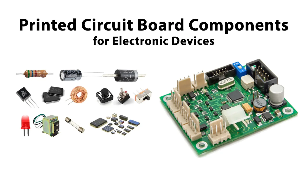
A printed circuit board (PCB) is an important component in almost all electronic gadgets . It works as a substrate for mounting electronic elements and offers adjoin paths for electrical signals. The printed circuit board includes layers of insulating product (like FR-4) with copper traces engraved to form circuits.
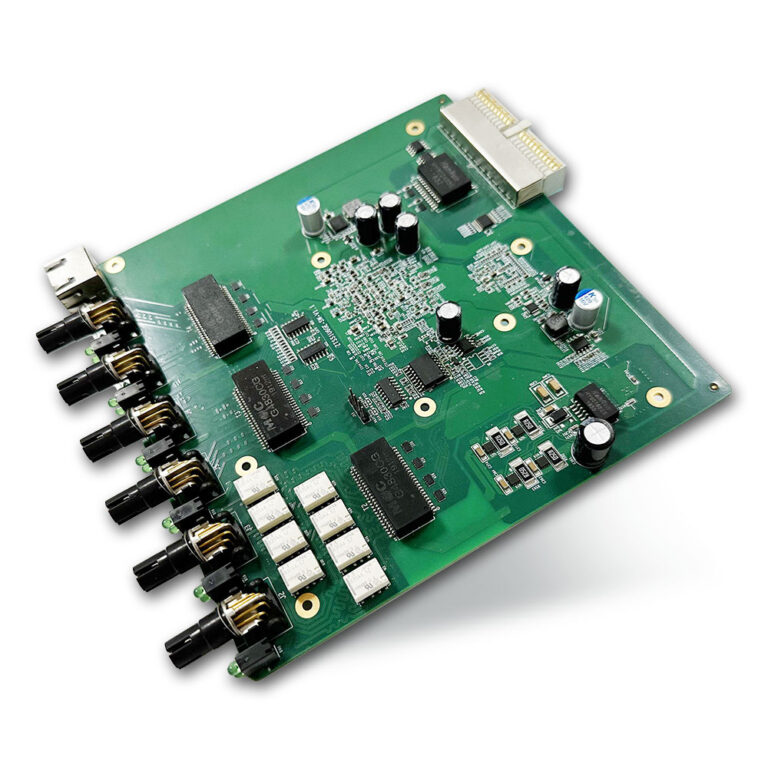
PCBs can be single-layer, double-layer, or multi-layer , depending on the intricacy of the electronic circuit . Single-layer boards are common in basic devices like calculators, while multi-layer PCBs are used in advanced systems like servers and integrated circuits . The role of a PCB is to make sure trusted connections between discrete parts such as resistors, capacitors, and integrated circuits .
The function of a PCB extends beyond electrical connection. It likewise supplies mechanical assistance for components and manages thermal conductivity to prevent overheating. Without a PCB , electronic gadgets would be undependable, large, and inefficient.
2. The Function of a PCB in Electronic Circuits
The function of a PCB is to act as a platform for electronic elements and to facilitate their interaction. By using copper layers and vias , a PCB makes it possible for exact routing of signals and power . This is important for control systems , consumer electronics , and high-speed applications like 5G networks.
A PCB also contributes in impedance matching , ensuring that signals travel effectively without distortion. For instance, in high-frequency circuits , the dielectric homes of the substrate and the spacing of copper traces figure out signal integrity. The solder mask layer safeguards the copper from oxidation and brief circuits, while part positioning enhances efficiency and heat dissipation.
In printed circuit board assembly (PCBA) , the PCB is occupied with elements by means of solder and surface-mount innovation . This procedure requires cautious design to prevent issues like crosstalk or thermal tension .
3. How Does a PCB Work? A Breakdown of Conductive Layers
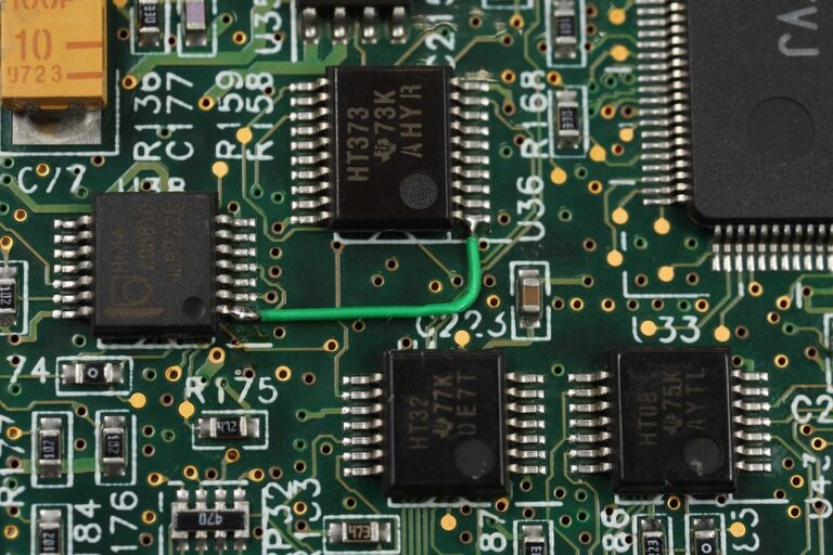
A PCB works by leveraging conductive products and insulating product to create a practical electronic circuit . The core of a PCB is a layer of copper foil laminated onto a substrate . This copper is then engraved to form traces — the conductive paths that link elements .
The conductive layers are separated by dielectric layers, which insulate them and avoid brief circuits. Vias (little holes plated with copper ) allow interconnect between various layers. For instance, a multi-layer PCB may have 4 copper layers stacked with dielectric material in between.
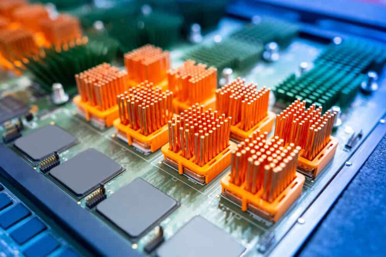
The thermal conductivity of a PCB is also critical. In high-power applications, metal-core PCBs or versatile PCBs are utilized to dissipate heat successfully. The printed circuit board acts as both a platform and a heat sink , ensuring the durability of electronic elements .
4. The Importance of PCB Style in Advanced Electronics
PCB design is a complex procedure that identifies the efficiency, dependability, and expense of an electronic device . Modern PCB style tools like Altium Designer make it possible for engineers to replicate circuit board design before manufacturing. This assists determine concerns like crosstalk or signal integrity early in the design procedure .
A new PCB design should account for part positioning , layer stack-up , and routing rules . For example, in high-speed PCBs , impedance and trace width are carefully calculated to minimize signal loss. The pcb layout likewise affects thermal management , making sure that elements do not get too hot.
PCB style solutions must stabilize performance with manufacturability . A badly created PCB can lead to defects during pcb production , increasing expenses and hold-ups. This is why design groups work together closely with pcb makers to enhance the design and manufacture procedure.
5. Secret Components of a PCB Layout and Stack-Up
The pcb design is the foundation of a printed circuit board . It defines the positions of components , copper traces , and vias . A well-designed design makes sure optimum efficiency and dependability .
The pcb stack-up describes the plan of copper layers and dielectric products. For instance, a 4-layer PCB might include 2 copper layers for power and ground , and two for signal routing . The stack-up impacts impedance , crosstalk , and thermal conductivity .
In rigid printed boards, the stack-up is repaired, while flexible PCBs enable dynamic setups. The solder mask and surface finish (like HASL or ENIG ) also contribute in safeguarding the copper and guaranteeing reliable soldering .
6. Obstacles in PCB Production Processes
PCB production includes several steps, including laminating , drilling , engraving , and soldering . Each step requires precision to prevent problems like short circuits or misaligned vias .
One challenge is microvia drilling for high-density interconnect (HDI) boards. These small vias demand advanced laser drilling and chemical etching methods. Another problem is conformal coating to safeguard parts from moisture and dust.
Additive production is revolutionizing pcb manufacturing by lowering waste and making it possible for complex 3D structures . Nevertheless, traditional subtractive methods (like engraving ) stay dominant in mass production .
7. How to Style a New PCB: A Step-by-Step Guide
Designing a brand-new PCB starts with developing a schematic using tools like Altium Designer . The schematic draw up element connections and power distribution .
Next, the pcb design is produced, where parts are placed and traces are routed. Rules for trace width , clearance , and by means of size are set to fulfill design specifications .
Lastly, the design is validated using DRC (Design Rule Inspect) and ERC (Electrical Guideline Examine) to catch errors. Once approved, the PCB is sent out for manufacture , followed by assembly and testing.
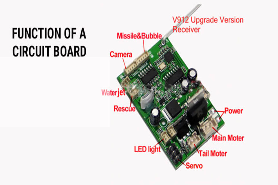
8. The Role of Process Control Block in PCB Operations
The process control block (PCB) is a concept from running systems , however its concepts apply to printed circuit board operations. Simply as a PCB in OS handles resources for a process , a printed circuit board handles resources for an electronic gadget .
In PCB manufacturing , a process control block might track parameters like temperature level , pressure , and chemical concentrations throughout engraving or laminating . This makes sure constant quality and compliance with design specifications .
9. Why PCBs Are Necessary for Consumer Electronics
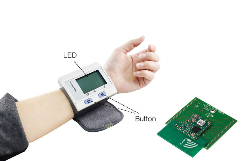
Customer electronics like mobile phones and smartwatches count on PCBs for density and performance. PCBs enable miniaturization by permitting high-density interconnects and multi-layer designs .
For instance, a smartphone PCB incorporates incorporated circuits , sensors , and antennas in an area smaller than a credit card. The thermal conductivity of the PCB guarantees the device stays cool throughout heavy use.
Without PCBs , consumer electronics would be bulky, inefficient, and susceptible to failure. PCB makers are constantly innovating to satisfy the needs of contemporary electronic devices .
10. Future Trends in PCB Technology and Innovation
The pcb industry is developing with trends like flexible PCBs , embedded parts , and green production . Flexible PCBs make it possible for bendable gadgets like collapsible phones, while embedded parts lower the need for discrete elements .
Advanced PCB innovations, such as 3D printing and additive production , are gaining traction. These approaches lower waste and allow custom PCBs for specific niche applications.
Sustainability is likewise a focus, with pcb manufacturers embracing lead-free solder and recyclable substrates . As AI and IoT drive demand for high-speed PCBs , development will remain essential to the electronics industry .