What's AOI Test (Automated Optical Inspection )?
Technical Principle
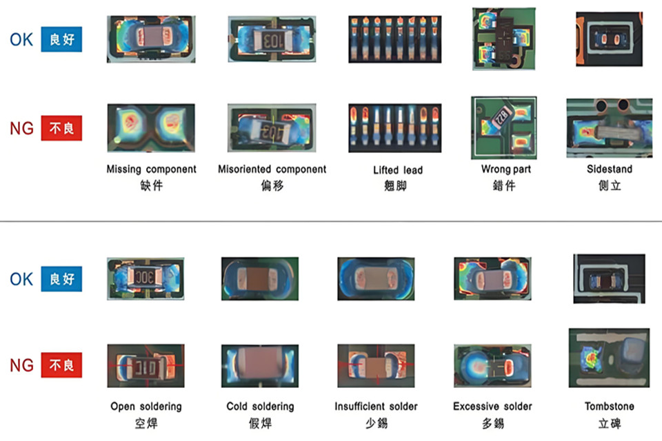
AOI Test through optical imaging + image algorithms , contrast PCB board line , components and pad with the database standard, accurate identification offset, short circuit, empty welding, leakage, reverse mount and other defects, to ensure that the quality of the PCBA product , to support the detection of the high-density HDI boards to large-size PCBs, and to provide online Real-time inspection program to improve production efficiency.
How AIO Test work ?
Principle of AOI technology: scientific logic of high-precision inspection
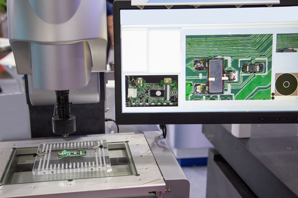
AOI Test carries out automated inspection of PCB boards through a high-speed, high-precision vision processing system. Its core process is as follows:
- Image Acquisition: Utilizing high-resolution camera or laser scanning technology, it quickly captures detailed images of PCB lines, component solder joints and pads.
- Parameter Comparison: Real-time comparison of the captured images with the preset qualification standards (such as solder joint size, positional accuracy, etc.) in the database.
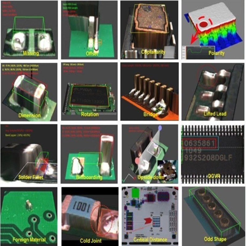
- Defect Identification: Identify potential problems through image processing algorithms (e.g. edge detection, pattern recognition), including common defects such as offset, short-circuiting, empty soldering, leakage soldering, more/less tin, reverse mount, and so on.
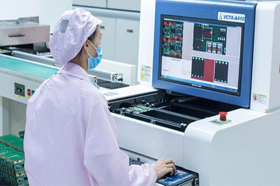
- Results feedback: through the display or automatic marking system, intuitively present the defect location, assisting maintenance personnel to quickly correct, reduce manual intervention errors
What the application of AOI Test ?
AOI Test application scenarios: covering the entire production line of quality guardian
AOI technology is widely used in electronics manufacturing, automotive electronics, semiconductors, new energy and other fields, especially in the following links play a key role:
- SMT (Surface Mount Technology) production line: detecting component placement accuracy, solder paste printing quality and reflow effect to ensure product consistency.
- PCB Bare Board Inspection: Covering fine-pitch high density boards (HDI) to low-density large-size boards, adapting to different process requirements.
- Online Inspection Solution: integrated in the production line, realizing real-time online inspection, significantly improving production efficiency and reducing the risk of defective product flow.
- Semiconductor Packaging Testing: Accurately identify tiny defects in wafer-level packages through multi-spectral imaging technology.
What core advanctage of AOI Test ?
The core advantages of AOI: high efficiency, precision, cost reduction and efficiency
Replaces manual visual inspection, improves consistency
AOI eliminates differences in human judgment through standardized inspection logic (Rule-based system), ensuring that each board meets the design specifications.High-speed inspection, matching the needs of Industry 4.0
Supports thousands of inspections per minute, adapting to high-capacity production lines and significantly shortening the quality inspection cycle.Early detection of defects, reduce maintenance costs
Identify problems early in the assembly process to avoid defective products flowing into subsequent processes, reducing scrap rates and rework costs. According to industry data, AOI can reduce product defective rate by more than 70%.AI-enabled, breaking through traditional limitations
Combined with AI algorithms (e.g., deep learning, image enhancement technology), AOI can autonomously learn defect features, cope with complex background interference, and reduce the leakage rate.
What trends of AOI test in Market ?
Industry trends: rapid growth of the AOI market and technological innovation
The global AOI test market size is expected to exceed 28 billion yuan in 2025, China as the world’s largest electronics manufacturing base, the penetration rate continues to increase. The following trends are worth paying attention to:
- Popularization of 3D AOI technology: more accurate solder joint height and shape inspection is achieved through 3D imaging to meet the demand for high-density interconnect (HDI) and BGA packaging.
- Multi-spectral and X-ray fusion inspection: for new energy batteries, semiconductors and other fields, to improve the ability to identify hidden defects (such as hole wall etching, diaphragm microvia).
- Accelerated localization: domestic equipment manufacturers in the field of consumer electronics market share of more than 60%, but high-end semiconductor testing is still dependent on imports, technological breakthroughs in the vast space.
Why US for the AIO test ?
AOI Test Inspection promise
high efficiency, precision, cost reduction and efficiency
1. High-precision inspection 0.01mm resolution
accurately identify PCB solder joint defects, improve product consistency.
2. Automation instead of manual labor
Reduces human error, realizes standardized quality inspection, and reduces labor cost by more than 30%.
3. Early Detection and Correction
Online real-time inspection, defect interception rate of more than 99%, to avoid the flow of defective products to subsequent processes.
4. AI Intelligent Upgrading
Deep learning algorithm optimizes the false alarm rate to 2%, adapting to complex processes and random defect identification.
5. Multi-Industry Coverage Automotive Electronics/Semiconductor/New Energy
Widely used in automotive electronics/semiconductor/new energy fields, supporting large-size to high-density board inspection.
6. Data-driven optimization
Defects classification statistics + SPC analysis, to provide the basis for process improvement, yield rate increased by 3% -5%.