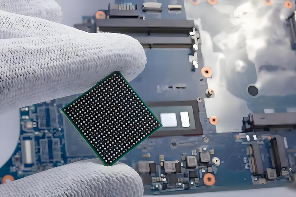
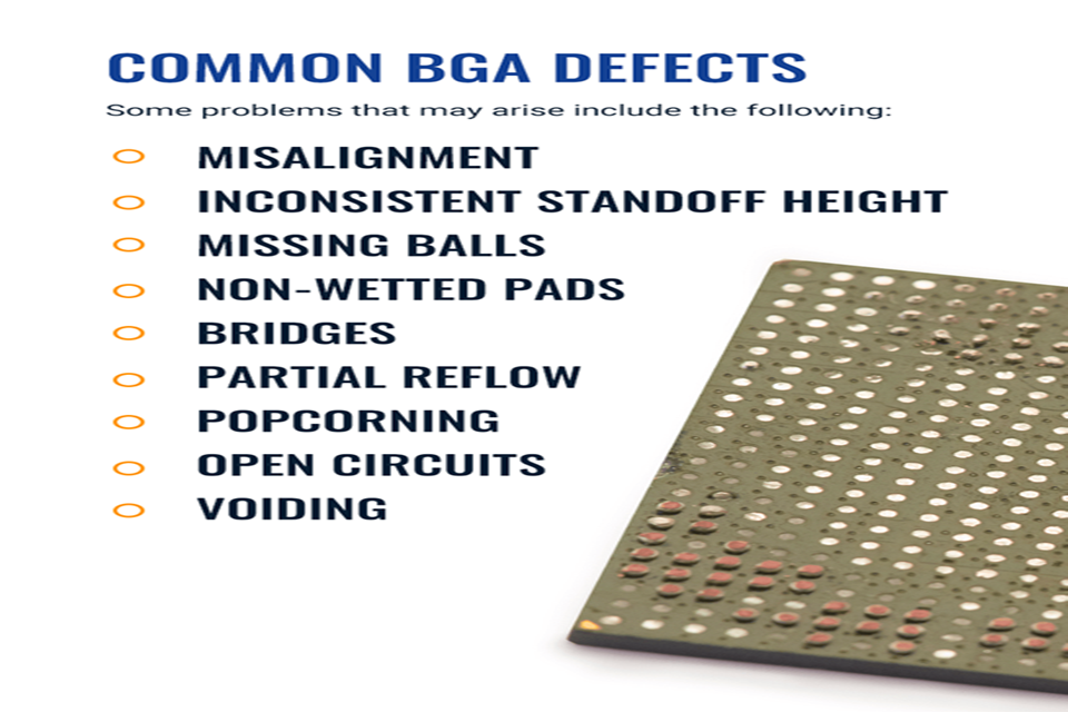
What is a BGA(Ball Grid Array)?
X-RAY Test is to test BGA,QFN and so on ,Ball Grid Array (BGA) packaging technology is a surface mounting technology used on integrated circuits. This technology is often used to permanently fix devices such as microprocessors. BGA packaging can provide more pins than other packages such as dual in-line packages or quad flat packages. The entire bottom surface of the device can be used as pins instead of only the periphery. It can also have a shorter average wire length than the periphery-limited package type to have better high-speed performance. Ball Grid Array (BGA) packaging is an array made at the bottom of the package substrate, and the solder balls are interconnected with the printed circuit board (PCB) as the I/O end of the circuit. The device packaged using this technology is a surface mount device. BGA (Ball Grid Array), referred to as BGA, is translated as spherical contact array packaging, and can also be translated as “ball grid array” or “network solder ball array” and “spherical array” and so on. It is a surface mount package for multi-pin LSI, in which spherical contacts are made in an array on the back of the substrate as pins and LSI is assembled on the front of the substrate (some BGA chips and lead ends are on the same side of the substrate).
What Features of Ball Grid Array(BGA)?
Here are the top 10 features of BGA packages:
- BGA package high I/O density, high frequency applications first choice
- BGA ball grid array strong heat dissipation performance, chip stability guarantee
- BGA package technology low parasitic parameters, signal transmission delay minimized
- BGA package thin and light, highly integrated space-saving
- BGA package process automated production, mass manufacturing low cost
- BGA package coplanar welding technology, reliability increase by 30
- BGA package anti-electromagnetic interference, high-speed communication excellent performance
- BGA package thermal management optimization, power consumption control more efficient
- BGA package supports high pin-count chips, graphics processor ideal choice
- BGA package is widely used in consumer electronics/server/automotive electronics.
What Type of Ball Grid Array(BGA)?
The following is a summary of the types, core advantages and disadvantages of BGA packaging.
BGA packaging types and core advantages
| BGA packaging types | Core advantages | Typical application scenarios |
|---|---|---|
| TBGA packaging | Flexible carrier, excellent thermal matching, economical choice | Consumer electronics low-cost solution |
| CBGA packaging | Ceramic substrate, high air tightness, strong long-term reliability | Military/aerospace high reliability scenarios |
| FCBGA packaging | Flip chip, high heat dissipation efficiency, anti-electromagnetic interference | High-performance computing/server |
| PBGA packaging | Plastic substrate, low cost, good thermal matching | Mid- and low-end consumer electronics |
| FBGA packaging | Fine pitch solder balls, high-density layout, suitable for memory chips | Storage controller/DDR memory |
| UFBGA packaging | Extremely fine solder balls, smallest size, excellent high-frequency performance | 5G communication/IoT chip |
BGA package advantages and disadvantages
| Core advantages | Key features | Data expression | Core disadvantages | Solution |
|---|---|---|---|---|
| High I/O density | High-frequency application | The number of pins exceeds 3 times of traditional packaging | Moisture sensitive | Moisture-proof packaging + reflow soldering process |
| Low parasitic parameters | Small signal transmission delay | Circuit stability improved by 40% | Complex process | High-precision equipment + automated production line |
| Lightweight design | Volume reduced by 50% | Save PCB space | Difficult rework | X-ray detection + special rework tools |
| High heat dissipation efficiency | Chip directly touches the air | FCBGA has the best heat dissipation performance | Thermal expansion difference | Thermal matching material optimization design |
| Automated production | Coplanar welding | Cost reduction of 30% | Higher cost | Bulk purchase + process optimization |
How the Ball Grid Array(BGA) soldered to PCB ?
The following is a summary of the core steps in soldering BGAs to PCBs, combined with information on high-density soldering techniques, temperature profile optimisation and more:
1. Pre-processing and alignment
Baking moisture removal: PCB and BGA need to 80-90 ℃ baking 10-20 hours to avoid welding bubbles.
Surface Cleaning: Remove PCB pad grease and oxidation layer with alcohol or board washing water to ensure solder paste adhesion.
Accurate alignment: by optical positioning or manual alignment of BGA around the silkscreen line, allowing 30% offset, the use of molten tin tension self-correction.
2. Solder Paste Printing & Fixing
Solder Paste Printing: Uniformly apply solder paste (lead-free/leaded) using a stencil with thickness and openings matching the BGA ball diameter.
BGA Fixing: Lightly press the BGA to the PCB, and prevent offsetting with the help of vacuum suction pen or bonder.
3. Reflow soldering control
Temperature profile: in three stages – preheating (3-5 ℃ / s heating), holding (uniform heat penetration), reflow (peak 220-235 ℃ molten tin).
Equipment selection: BGA rework workstation or reflow oven with hot air nozzles to cover the edge of the chip to avoid local overheating.
4. Cooling and Inspection
Slow cooling: Natural cooling rate 3-10°C/s to prevent solder joint cracking or PCB deformation.
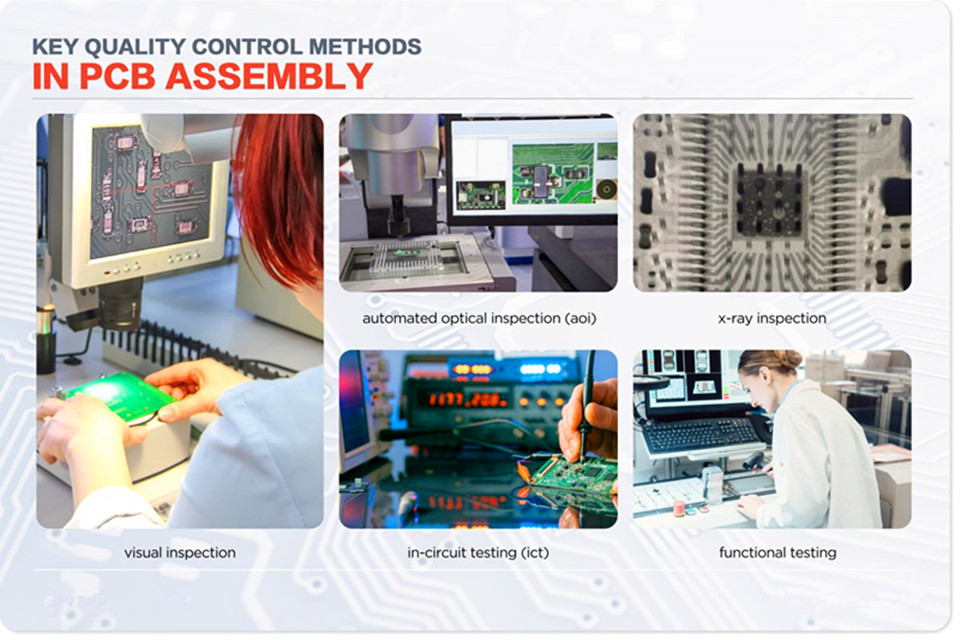
Quality Verification: X-ray fluoroscopy of solder joint structure, AOI inspection of appearance, functional test to ensure electrical connection.
Optimised solution
Anti-interference design: TBGA flexible substrate is preferred for high-frequency scenarios to reduce signal loss.
Heat dissipation enhancement: FCBGA flip chip + thermal conductive adhesive filling to enhance the heat dissipation efficiency of high power devices.
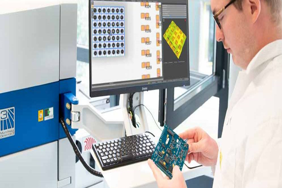
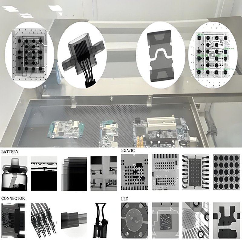
What is X-RAY Test ?
X-RAY Test is a mature non-destructive test method that uses low-energy X-RAY Test to detect the internal structure and quality of the object being done without damaging it. This method is widely used in the industrial sector, especially in testing electronic components, semiconductor packaging products, printed circuit boards, etc.
Finding non-destructive internal defects
– low-energy X-rays PCB/semiconductor reveals defects without loss.Variety for diverse packages
- DIP/SOP/QFN/BGA/Flipchip Analysis for electronic components .
Comprehensive tests in stages
- IQC/FA/QC/QA/R&D Workflows With detection of automatic defects .
Advanced 3D imaging for accuracy
- Semcover packaging and PCB bare board inspected at Micro-Level .
Important for high-value industries
- Automotive/aerospace/medical system are valid with zero-failure standards .
Cost-skilled defect detection
– IGBTS/LED/Li-ion battery Tested for long-term reliability .Aluminum Casting Non-Business Tests
- Metal component integrity verified with X-ray density maps .
How Does PCBX-RAY Test Work?
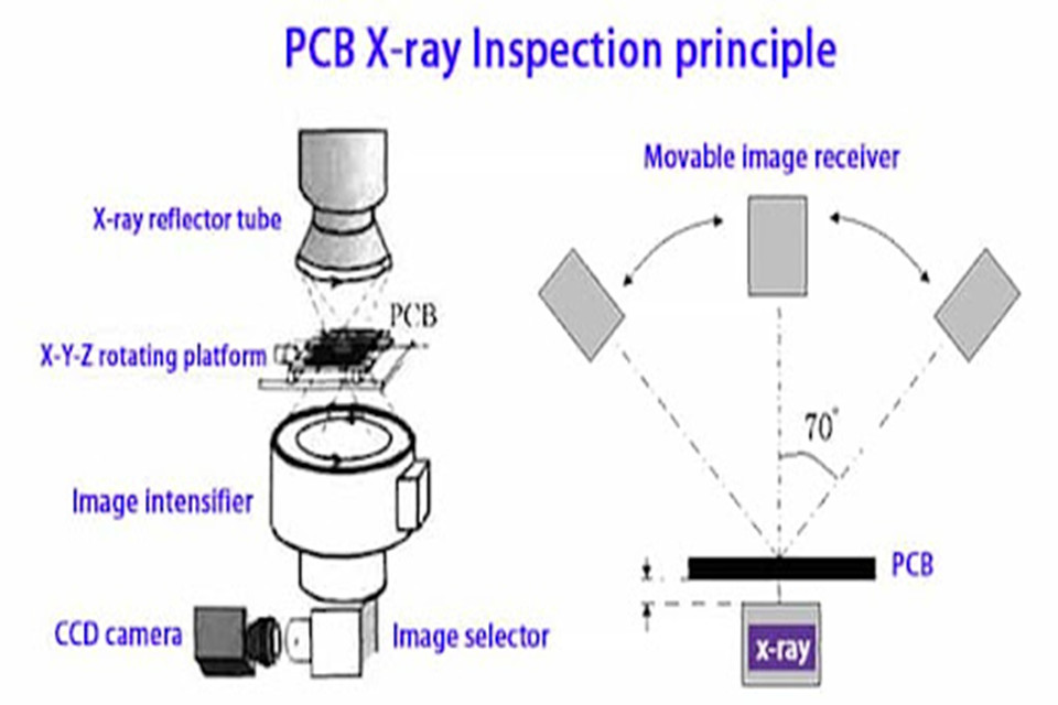
How X-RAY Test works?
X-RAY Test obtains non-destructive tests through X-ray penetration and material absorption difference. Its main process is as follows:
X-ray generations: X-ray sources (such as X-ray tube) testing the object being tested emit high-energy X-rays under high pressure
Material absorption and imaging:The content of different density or thickness has different absorption rates for X-rays (for example: metals absorb more, plastic less absorbing). X-rays that have entered are obtained by the detector to create an opposite image (similar to “shadow”), which reflect the internal structure of the object.
Defect Identification:The image processing system analyzes the opposite difference and identifies internal defects (such as mixed voids, cracks, defects, etc.). -The high-resolution equipment combined with AI algorithm can automatically mark defects and generate reports.
Application landscape:
- Electronic manufacturing: Find BGA/QFN solder balls, PCB solder joints and 3D packaging structures.
- Industrial Inspection: Check metal casting, welded joints and aerospace components.
- Anti-counterfiting: Identify fake by comparing internal structural differences between real and fake components.
Features:
- Non-destructive: No need to disassemble samples to protect high-value products.
- Efficient and accurate: Complex structure inspection can be completed in a single scan, and the defect identification accuracy can reach the micron level.
- Multi-dimensional analysis: Supports 2D imaging and 3D tomography (CT technology) to meet different inspection needs.
2D X-RAY Test VS 3D X-RAY Test Comparison summary
| Dimension | 2D X-RAY Test | 3D X-RAY Test |
|---|---|---|
| Image type | Planar projection | 3D reconstruction model |
| Defect location | Single-direction projection, possible occlusion | Multi-angle analysis, accurate positioning of defect positions |
| Applicable scenarios | Simple structure, fast screening | Complex structure, high-precision detection |
| Cost and efficiency | Low cost, fast detection speed | High cost, long time |
Typical applications:
- 2D: BGA solder joint short circuit detection, QFP pin offset.
- 3D: Chip stacking defects, micron-level pore analysis.
What Key Benefits of X-RAY Test?
Why choose X-RAY Test for PCB manufacturing and PCB Assembly ?
Apply hidden PCB defects
- Find out Solder Voids , Missalignaments , and Bizing In real time.
- Identify internal cracks in multi-layer PCB with accuracy.
Complex PCB QA Revolution
- Inspection High density PCB and short components effectively.
Copy Multi-Lear Board Assembly with a waging test.
- Inspection High density PCB and short components effectively.
Reduce product failure risk
- Stop field failures and reputation damage with initial defect detection.
- Ensure Safety-Critical Systems Complete reliability standards.
Cost reduction with early detection
- Less scrap rates and rework cost through active inspection.
- Adaptation Production Efficiency and Yield Improvement .
Increase AOI limits
- Look beyond AOE Blind Spot with 360 ° visibility of X-rays.
- Analysis solder paste height and zero percent automatically.
Future-proof your production
- BGA/QFN/Flipchip and adapt to advanced packaging trends.
-Milia IPC-A-610 and jedec originally to compliance standards.
- BGA/QFN/Flipchip and adapt to advanced packaging trends.
Solving the quality problems of BGA, QFN, 3D packaging and counterfeit components
BGA/CSP solder ball integrity analysis
QFN leadframe alignment verification
Embedded component validation
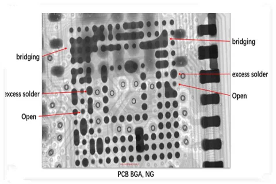
What Common Defects Identified by X-RAY Test?
- Detect a variety of package components, such as BGA/QFN/Flipchip, with strong applicability.
- Observe the chip stacking die structure, clearly present the internal layout and binding lines.
- Accurately identify package defects, such as chip cracks, bubbles, cold solder joints.
- Penetrating AOI blind area detection, making up for the limitations of optical detection, comprehensive and efficient.
- Analyze internal defects of products, such as abnormal welding of electronic components, with strong visualization.
- Automatically measure the bubble ratio, AI intelligent judgment, accurate and reliable results.
- Quantify DIP creep height, standardize evaluation, and improve process consistency.
- High-definition imaging defect analysis, assist failure location, and support data traceability.
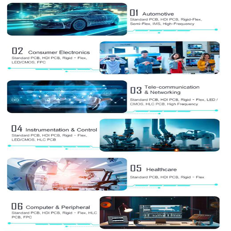
What Applications of X-RAY Test Across Industries?
1.Aerospace: Detect Counterfeit Parts
- Ensure military-grade PCB compliance (AS9100/MIL-STD).
- Mission-critical system validation with 3D X-Ray imaging.
Automotive: Validate Safety Systems
- Airbag controller inspection for zero failure risk.
- Harsh-environment PCB testing in EVs and ADAS.
Consumer Electronics: Boost Reliability
- High-density PCB QA for smartphones/tablets.
- Wearable tech defect detection in compact designs.
Medical Devices: Lifesaving Accuracy
- FDA-compliant implantable device validation.
- ECG/ventilator PCB inspection with sub-micron precision.
Telecom: 5G Infrastructure Assurance
- High-frequency PCB testing for 5G base stations.
- Multi-layer board integrity in network gear.
Industrial: Harsh-Environment Solutions
- Oil & gas equipment X-Ray for subsea sensors.
- Renewable energy PCB validation (solar/wind inverters).
Why X-RAY Test is Essential for Every Industry
How to Choosing the Right X-RAY Test?
5 major factors to choose your X-RAY Test partner
Ensure quality-driven manufacturing with the provider of non-destructive tests and accurate defects for mission-critical electronics.
Choosing the Right X-RAY Test
1. 🔍 submine resolution and 3D CT scanning
Copy multi-layer PCB integrity with <2.5μm accuracy and BGA zero analysis. Priority to the system offering:
• Automatic 2.5D/3D Tomography
• High density component handling
• IPC-610 certified inspection
2. 🛡 Industry-specific expertise
Demand aerospace-grade verification and motor vehicle QC protocol. Please attest it:
• 10+ years in Medical/5G PCB test
• ISO 13485 and IATF 16949 compliance
• BGA/CSP Dosha Libraries
3. ⏱ Rapid turnaround and scalability
Opt for the same day analysis and high-volume batch processing. to ensure:
• <5-minute/panel scan speed
• 24/7 production line support
• Customable throwput
4. 📊 AI-Powered Dosha Analytics
Leverage automatic zero% calculation and real time process reaction. key features:
• IPC-7095 obedient reporting
• Cloud-based data integration
• Root-causing failure map
5. 🤝 ROI- Customer Assistance
Select partners offering 24/7 technical guidance and free process audit. Priority:
• Representation services on site
• BGA Rework Optimization
• Life maintenance plans
Why US for your X-RAY Test partner ?
Why Choose SevenPCBA for X-RAY Test?
Technical expertise
- Aerospace/Defense QA for 3D X-Ray Imaging
- BGA/QFN Dosha Analysis for 2.5D/3D CT Scanning
- AS9100/ISO 9001 certified Non-destructive test
Quality Assurance
- To detect high-resolution defects in PCB and semiconductors
- R&D-grade report With automated defect classification
- Customized solution for high-lecracy production qa
Customer Success Highlights
- 35% area failure reduction Aerospace for customers
- 100% FDA Compliance For medical equipment manufacturers
- Warranty Claims Prevention BGA Dosual through Identification
- Automotive electronics verification With zero-failure standards
- Semiconductor Packaging QA 5G Network Components
- Cost-skilled mass production With AI-Powered Insight