-
Xinxintian Industrial Zone, Shajing Street,Bao'an District, Shenzhen, China
What is PCB Assembly (PCBA)? A Comprehensive Explanation
Abstract: .
This short article provides a detailed explanation of PCB Assembly (PCBA) , the vital production process that transforms a bare Printed Circuit Board (PCB) into a practical electronic module. We detail the actions involved, from part sourcing and solder paste application to part positioning, soldering, and strenuous screening. The discussion highlights essential technologies like Surface area Mount Technology (SMT assembly) and Through-Hole Innovation (THT), stressing their functions in modern electronics production. The goal is to use a clear understanding of PCBA’s significance in producing the electronic devices we utilize daily.
Introduction .
In the realm of modern electronic devices, the Printed Circuit Board (PCB) acts as the foundational platform. However, a bare PCB is merely a substrate with conductive pathways. It requires a sophisticated process referred to as PCB Assembly (PCBA) to end up being the heart of an electronic gadget. This process includes thoroughly mounting and interconnecting numerous electronic parts onto the PCB . This post delves into the intricacies of PCB assembly , describing its core concepts, approaches, and critical value in the electronics making ecosystem. We aim to provide a clear, technically precise summary of how a bare board evolves into a fully operational electronic assembly.
Specifying PCB Assembly (PCBA): The Core Process .
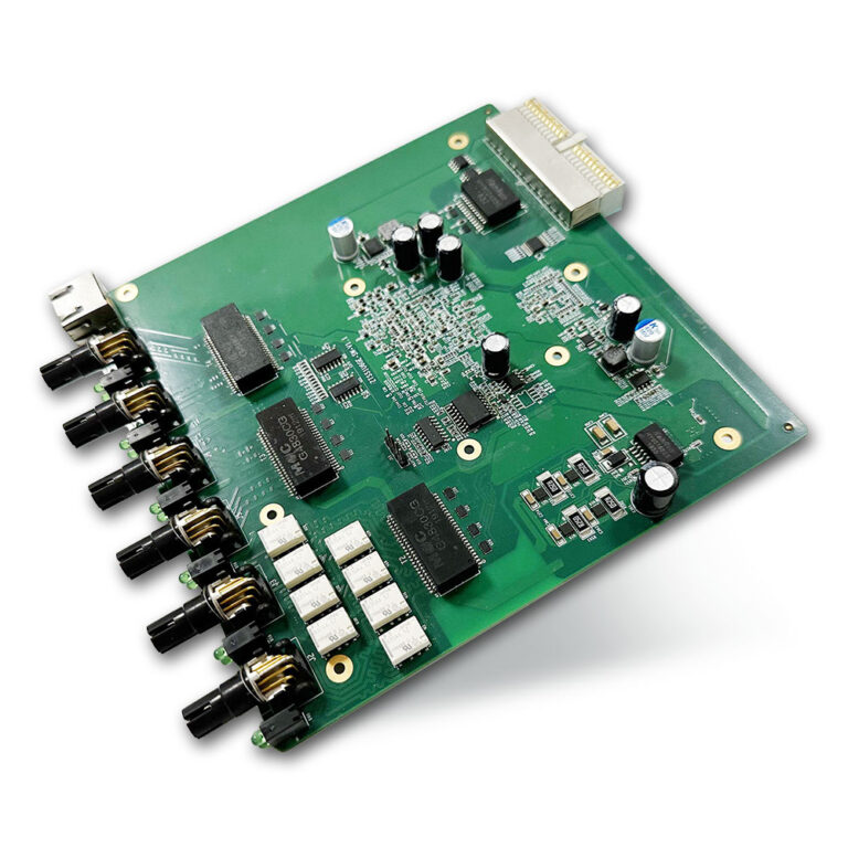
PCB Assembly , frequently abbreviated as PCBA , describes the thorough set of operations that populate a Printed Circuit Board (PCB) with electronic parts . This complex procedure changes a passive PCB into an active, practical circuit assembly. Engineers and professionals strategically put and solder parts such as resistors, capacitors, incorporated circuits (ICs), and connectors onto the PCB . This guarantees the correct electrical connections and mechanical stability, enabling the board to perform its desired electronic functions. PCBA is a foundation of electronics manufacturing, pivotal for producing everything from simple gizmos to intricate industrial machinery.
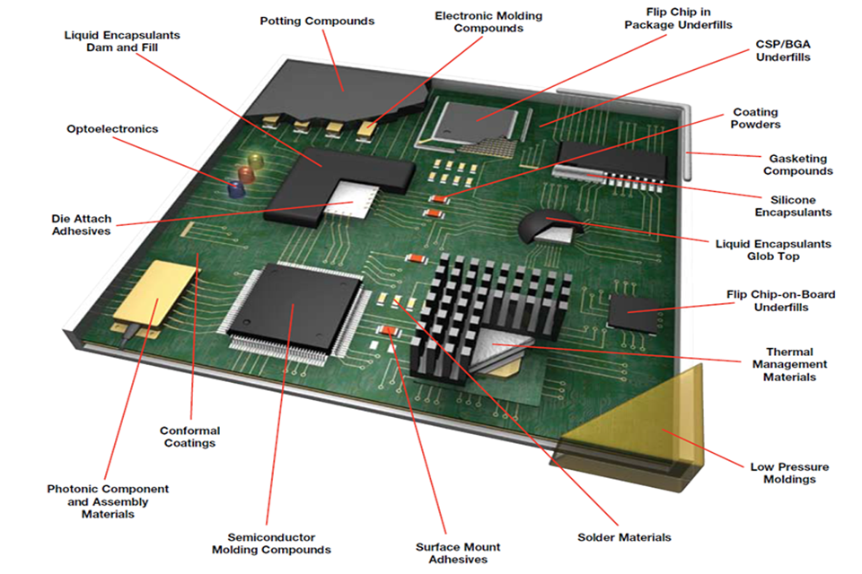
Essential Elements: The PCB and Elements .
The PCB assembly process relies on 2 primary constituents:.
- Printed Circuit Board (PCB): This is a non-conductive substrate, usually made from materials like FR-4 (a flame-retardant epoxy laminate). Makers engrave or print conductive paths, usually copper traces, onto its surface area( s). These pathways specify the electrical affiliations between parts. PCBs can be single-sided, double-sided, or multi-layered, depending on the circuit’s intricacy.
- Electronic Parts: These are the private active and passive gadgets that perform different electronic functions. Examples consist of:.
- Resistors: Limitation present flow.
- Capacitors: Shop electrical charge.
- Inductors: Shop energy in a magnetic field.
- Diodes: Permit present flow in one direction.
- Transistors: Magnify or switch electronic signals.
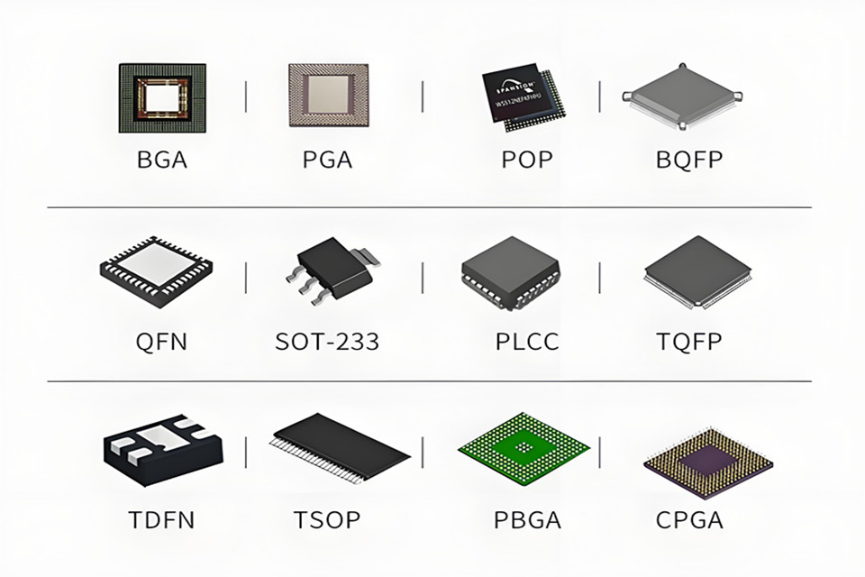
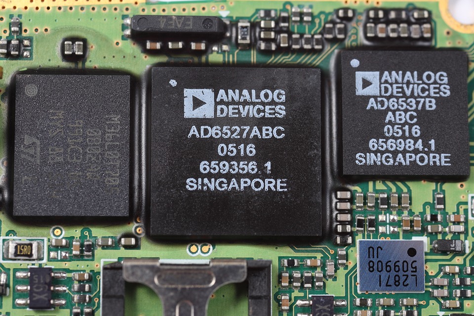
- Integrated Circuits (ICs): Complex circuits miniaturized on a semiconductor chip, carrying out varied functions (e.g., microprocessors, memory).
- Connectors: Help with electrical connections to other boards or external devices.
( New Section 1) .
Secret Phases in the PCB Assembly Workflow .
The PCB assembly journey involves a number of unique, yet adjoined, phases. Precision and control at each action are vital for attaining a premium final product.
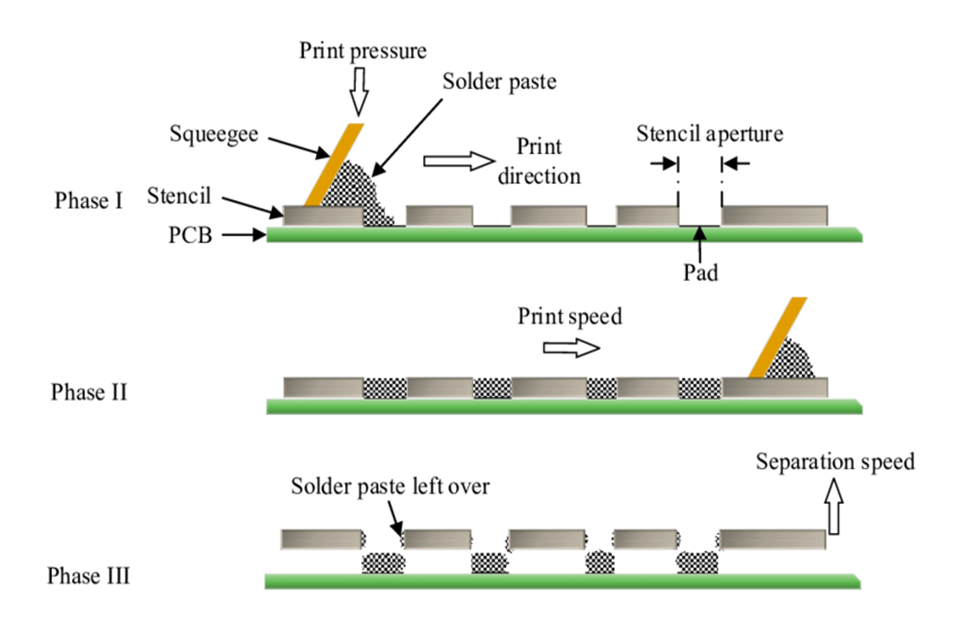
- Solder Paste Application: For SMT assembly , this is usually the initial step. Specialists apply an exactly regulated amount of solder paste to the PCB pads where surface install components (SMCs) will sit. They typically utilize a stencil (a thin metal sheet with laser-cut apertures) and a squeegee to ensure consistent deposition. The solder paste is a mixture of small solder particles and flux, which assists in the soldering process.
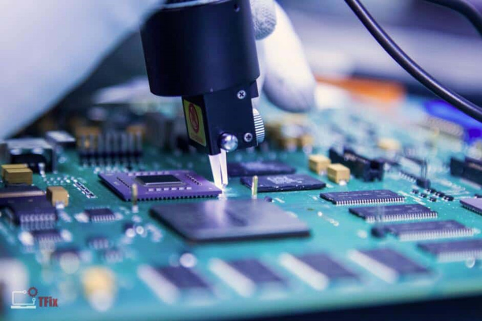
- Component Placement: Automated pick-and-place machines perform this phase with impressive speed and precision. These devices pick electronic parts from reels or trays and precisely position them onto their designated places on the PCB , guided by pre-programmed collaborates. This is particularly critical for high-density SMT assembly .
- Soldering: This stage produces the long-term electrical and mechanical connections.
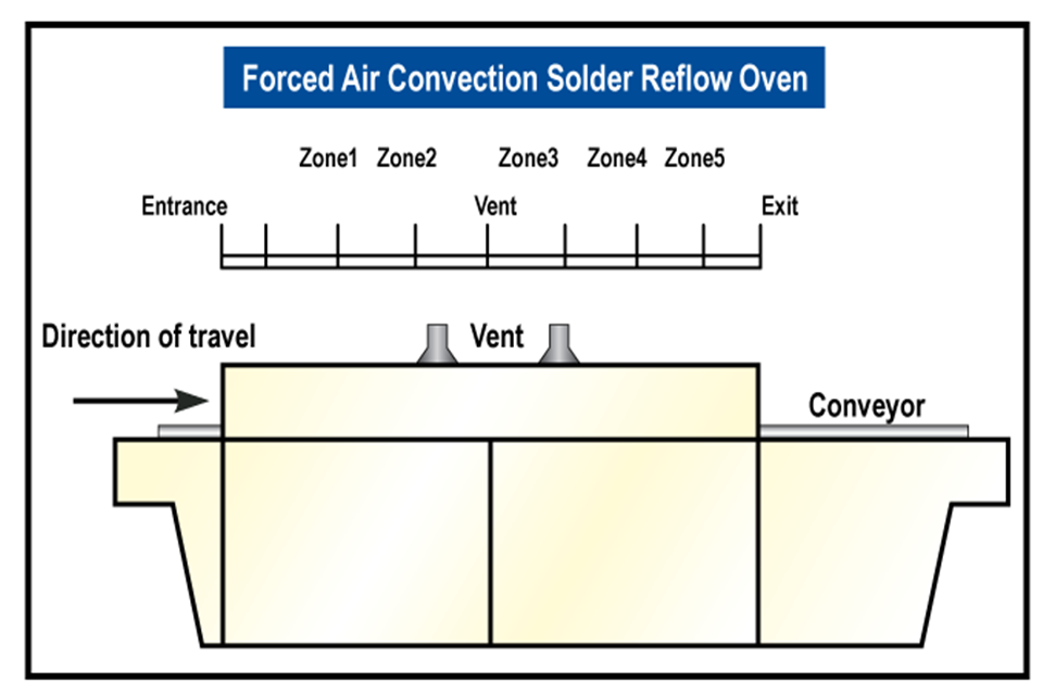
- Reflow Soldering (for SMT): After element positioning, the PCBs pass through a reflow oven. The oven subjects the boards to a carefully managed temperature profile, melting the solder paste and forming robust solder joints.
- Wave Soldering (mostly for THT): For Through-Hole Technology parts, or in some cases for mixed-technology boards, wave soldering is common. The PCB passes over a wave of molten solder, which solders the part leads extending through the board.
- Selective or Hand Soldering: Some components may require manual soldering or specific selective soldering strategies due to their level of sensitivity or placement.
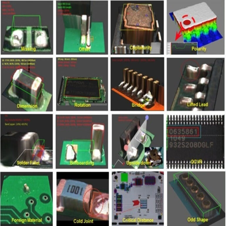
- Evaluation and Cleansing: Post-soldering, manufacturers inspect the boards for flaws. This can involve visual inspection, Automated Optical Examination (AOI), and X-ray evaluation (AXI) for elements like BGAs (Ball Grid Arrays) where solder joints are hidden. Cleaning might also be performed to eliminate flux residues that might cause deterioration or electrical issues.
- Testing: Technicians conduct different tests, such as In-Circuit Screening (ICT) and Functional Evaluating (FCT), to verify the PCBA functions as created.
( New Area 2) .
Quality Control and Screening in PCBA: Guaranteeing Reliability . Guaranteeing the reliability and performance of the last PCBA is vital. Robust quality assurance (QC) procedures and extensive screening protocols are integrated throughout the PCB assembly procedure .
- Inbound Quality Control (IQC): Manufacturers examine all raw materials, including bare PCBs and electronic parts , to ensure they meet specs before assembly begins.
- In-Process Quality Assurance (IPQC): Monitoring key criteria throughout assembly, such as solder paste volume, placement precision, and soldering temperature levels, assists find and correct issues early.
- Automated Optical Assessment (AOI): AOI systems utilize cameras to immediately scan PCBAs for flaws like missing components, incorrect polarity, solder bridges, and insufficient solder. This is a quick and effective approach for SMT assembly assessment.
- X-ray Assessment (AXI): For elements with hidden solder joints, such as Ball Grid Arrays (BGAs) and Quad Flat No-leads (QFNs), AXI supplies a non-destructive method to check joint integrity.
- In-Circuit Test (ICT): ICT checks private components on the populated PCB for shorts, opens, and correct worths, validating the stability of the assembly at the part level.
- Practical Test (FCT): This test mimics the last operating environment of the PCBA to ensure it performs its designated functions according to requirements.
These rigorous QC and screening actions decrease defects, enhance yield rates, and guarantee the long-term performance of the electronic device.
Core Assembly Technologies: SMT and THT .
Two primary technologies dominate the PCB assembly landscape:.
- Surface Area Mount Technology (SMT Assembly): . This strategy includes installing electronic components , known as Surface Mount Gadget (SMDs), directly onto the surface area of the PCB . SMDs have little leads or solder balls that reach solder pads on the board. SMT assembly permits greater element density, smaller board sizes, and is highly amenable to automation. It is the dominant innovation for a lot of contemporary electronic devices due to its effectiveness in high-volume production and viability for miniaturized styles. The SMT pcb assembly process usually consists of solder paste printing, high-speed element placement, and reflow soldering.
- Through-Hole Technology (THT): . In THT, element leads are inserted through pre-drilled holes in the PCB . Technicians then solder these cause conductive pads on the opposite side of the board, often utilizing wave soldering or hand soldering. While older, THT remains pertinent for elements needing greater mechanical strength (e.g., big adapters, transformers) or those not available in SMD plans. Many PCBs make use of a mix of both SMT and THT components.
( Optional Table) .
Comparison of SMT and THT Assembly .
| Function | Surface Mount Technology (SMT) | Through-Hole Innovation (THT) |
|---|---|---|
| Element Positioning | On PCB surface | Through drilled holes in PCB |
| Soldering Process | Reflow soldering | Wave soldering, hand soldering |
| Part Density | High | Lower |
| Automation Level | Very High (ideal for SMT assembly ) | Moderate |
| Mechanical Strength | Moderate | High |
| Board Size | Smaller sized | Can be larger |
| Suitability | Miniaturized, high-density designs, high-frequency applications | Robust connections, bigger parts, power applications |
| Cost (High Volume) | Generally lower for SMT assembly | Can be higher due to manual actions |
The Relevance of PCB Setting Up in Electronics .
PCB Setting up is not merely an action; it is the essential bridge between electronic design and a substantial, working item. Without precise and dependable PCBA , also one of the most fantastic circuit design would stop working to operate.
- Functionality Understanding: PCBA converts layout schematics into physical fact, producing the electric paths and connections that allow existing to flow and elements to connect as meant.
- Item Dependability: The high quality of PCB setting up straight affects the reliability and life-span of an electronic gadget. Appropriate soldering, part positioning, and handling prevent premature failures.
- Miniaturization and Intricacy: Advances in SMT setting up have made it possible for the development of significantly smaller, extra effective, and feature-rich digital tools.
- Foundation for Advancement: Reliable and cost-efficient PCBA solutions encourage trendsetters to bring new electronic products to market quickly.
Regularly Asked Concerns (Frequently Asked Questions) .
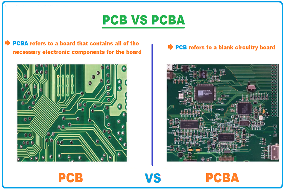
- What is the distinction in between a PCB and a PCBA? . A PCB (Printed Circuit Board) is the bare, uninhabited board consisting of conductive tracks and pads. A PCBA (Printed Circuit Board Assembly) is a PCB that has actually been inhabited with all the needed digital components with the setting up procedure, making it a useful electronic circuit.
- Why is SMT assembly widely favored in contemporary electronics? . SMT assembly allows for greater element density, enabling smaller and lighter products. It is extremely automated, resulting in quicker manufacturing rates and reduced prices in high-volume production. SMDs likewise usually offer better efficiency for high-frequency applications.
- What are some usual issues found during PCB setting up inspection? . Common problems consist of solder bridges (undesirable connections in between solder joints), open circuits (missing out on connections), not enough or extreme solder, element misalignment, incorrect element polarity, missing elements, and cool solder joints.
- How does solder paste work in the SMT setting up procedure? . Solder paste is a blend of tiny solder alloy fragments and flux. The change cleanses the surfaces to be soldered and protects against oxidation. Throughout reflow soldering, the solder bits thaw and fuse, producing solid metallurgical bonds in between the part leads and the PCB pads.
- Is hand-operated PCB setting up still appropriate today? . Yes, hand-operated PCB setting up is still appropriate for prototypes, tiny manufacturing runs, rework, fix, and for putting together specialized or THT parts that are not conveniently handled by automated equipment.
- What are the main obstacles in accomplishing top quality PCB assembly? . Secret challenges include taking care of increasingly smaller sized part sizes (like 0201 or 01005 plans), making certain solder joint stability for complicated packages (e.g., BGAs), managing the process for lead-free soldering (which calls for greater temperatures), stopping electrostatic discharge (ESD) damage, and handling intricate supply chains for electronic components .
Recap .
PCB Setting Up (PCBA) is a vital and very sophisticated process in the electronic devices sector. It carefully integrates electronic elements with a Printed Circuit Board (PCB) , changing it right into a functional device that powers many tools. From initial solder paste application in SMT assembly to the precise placement of elements and durable soldering strategies, each step needs accuracy and control. The choice between Surface area Mount Technology (SMT setting up) and Through-Hole Technology (THT), or a mix thereof, relies on details style needs, component kinds, and manufacturing volumes. Ultimately, top quality PCBA makes certain the efficiency, reliability, and durability of electronic items, making it an essential proficiency for any type of electronics producer. Recognizing the subtleties of PCB assembly is basic to appreciating the intricacy behind the digital gadgets essential to contemporary life.