10 أنواع شائعة من أعطال المكونات الإلكترونية الموجودة على لوحات الدوائر المطبوعة (PCBs)
خلاصة
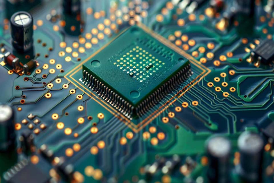
Electronic components on لوحات الدوائر المطبوعة (PCBs) can fail for several reasons, which affect the overall functionality and reliability of electronic devices. PCB have10 common types of electronic component failures based on detailed industry insight here.
جدول المحتويات
1. Overheating/ Thermal Failure
This is one of the most common failure settings, where an element runs over its optimum rated temperature level, bring about irreversible damages or considerable decrease in its lifespan.
- ملخص: Excessive warm degrades the semiconductor materials, thaws inner links, or damages the component’s packaging. The failure can be immediate (fatigue) or steady (accelerated aging).
- Common Causes: .
- Excessive Current: Drawing extra existing than the element is ranked for.
- Poor Thermal Monitoring: Inadequate heatsinking, poor air movement, or thick element placement that develops hot spots.
- High Ambient Temperature Level: The atmosphere the device runs in is as well warm.
- Affected Components: Power regulators, MOSFETs, high-power resistors, processors (CPUs/GPUs), and diodes.
- تجنب: Proper heatsinking, use followers, excellent PCB layout for air movement, and derating (running parts well listed below their optimum defined restrictions).
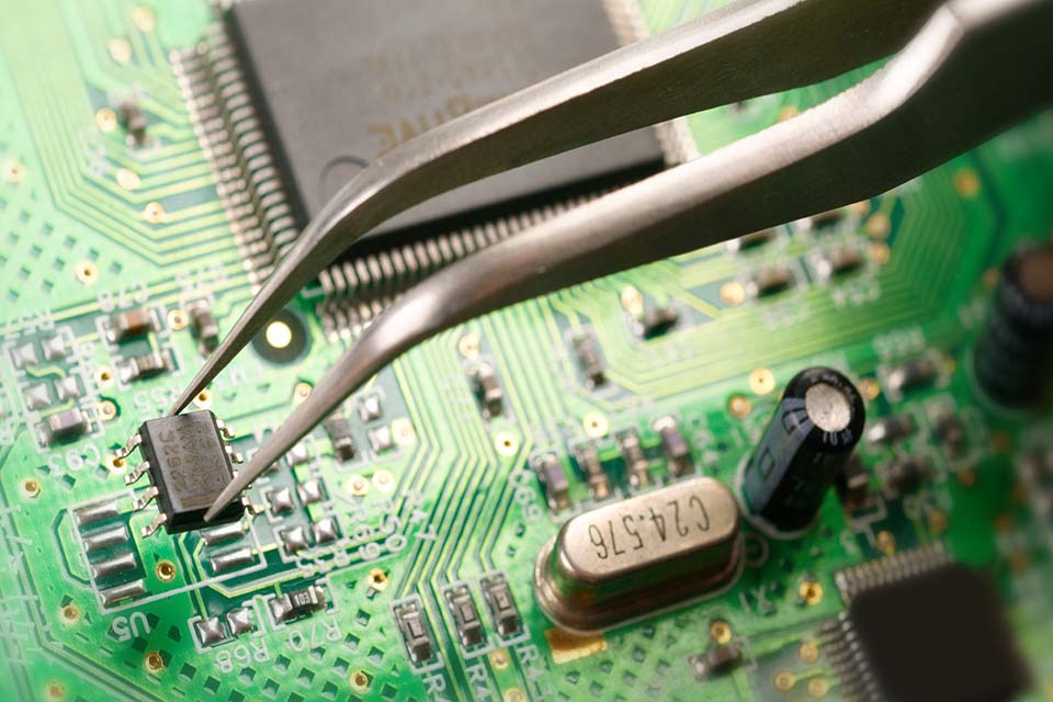
2. Solder Joint Failure
This is a mechanical failure of the link between the component and the PCB, instead of the component itself, but it makes the part non-functional within the circuit.
- ملخص: The solder joint splits or breaks, developing an open circuit or an intermittent connection that is usually challenging to detect.
- Usual Reasons: .
- Thermal Biking: The board and parts expand and agreement at different prices, emphasizing the solder joints over time. This is a main root cause of failing in devices utilized in varying temperature environments.
- Resonance and Mechanical Shock: Physical stress and anxiety from going down the tool or from consistent resonance can tiredness the solder.
- Poor Soldering Process: Cold joints, inadequate solder, or gaps produced during manufacturing.
- Affected Components: All surface-mount (SMT) and through-hole (THT) components, especially large or heavy ones like Round Grid Arrays (BGAs) and ports.
- تجنب: Proper control of the soldering process (temperature profiles), making for mechanical security, and using underfill or staking for elements in high-vibration atmospheres.
3. Electrical Overstress (EOS) and Electrostatic Discharge (ESD)
These are two associated yet distinctive kinds of electric damage brought on by revealing an element to a voltage or current past its requirements.
- Description: .
- EOS (Electric Overstress): A sustained direct exposure to too much voltage or existing (e.g., linking a 3.3 V chip to a 5V supply). This typically causes catastrophic exhaustion.
- ESD (Electrostatic Discharge): A really brief, high-voltage occasion (e.g., a static shock from human touch). It can puncture the delicate gate oxides in incorporated circuits, creating instant or concealed failing.
- Common Reasons: Power surges, inaccurate power supply, lightning strikes (for EOS); inappropriate handling without basing straps, and static build-up in automated assembly processes (for ESD).
- Influenced Components: Delicate ICs (cpus, memory), MOSFETs, and LEDs are particularly susceptible.
- وقاية: .
- For EOS: Making use of security tools like merges, varistors, and TVS (Transient Voltage Suppression) diodes.
- For ESD: Implementing appropriate ESD-safe taking care of procedures (wrist bands, anti-static floor coverings, based workstations) and creating in on-board ESD defense circuits.
4. Rust and Contamination
This is a chemical failing setting where conductive surface areas are weakened by direct exposure to dampness and pollutants.
- ملخص: Chain reaction on element leads, pads, or traces cause oxidation or various other types of corrosion, bring about inadequate conductivity, periodic links, or short circuits.
- Typical Reasons: .
- Exposure to Moisture and Dampness: Operating the device in a moist setting.
- Aggressive Change Residue: Flux used throughout soldering is not properly wiped the board and absorbs wetness from the air.
- Direct exposure to Chemicals: Spills or operation in a destructive ambience.
- Impacted Components: Connectors, element leads, and revealed copper pads.
- تجنب: Completely cleaning the PCB after assembly (de-fluxing), applying a تشطيب مطابق to seal the board from the environment, and using covered rooms (IP-rated).
5. Part Aging and Specification Drift
Parts are not excellent and their material properties alter in time and with use, causing them to wander out of their specified resistance.
- Description: A part’s key electric characteristic (e.g., resistance, capacitance) progressively adjustments until it is no longer within the array required for the circuit to function appropriately.
- Usual Reasons: Natural degradation of materials over an element’s operational life. Warm and electric stress and anxiety can accelerate this process.
- Influenced Components: .
- Electrolytic Capacitors: The electrolyte can dry out, creating capacitance to decrease and ESR (Matching Collection Resistance) to boost. This is an extremely typical factor of failing in power products.
- Resistors: Their resistance value can drift over time.
- Crystal Oscillators: Their frequency can drift, affecting timing-critical circuits.
- تجنب: Making use of high-grade, long-life elements, derating to decrease tension, and developing circuits that are forgiving of minor specification adjustments.
6. Dendritic Growth/ Electromigration
This is a specific and dangerous kind of short-circuit failure pertaining to contamination.
- Description: Drunk of a DC voltage and in the existence of wetness, steel ions migrate throughout the surface area of the PCB, developing tiny, conductive filaments called dendrites. These dendrites can expand between surrounding pads or traces, producing a short circuit.
- Typical Reasons: A mix of high moisture, ionic contamination (like flux deposit), and a relentless DC voltage bias in between 2 carefully spaced conductors.
- Influenced Parts: Locations with fine-pitch parts (like microcontrollers) and high-density formats are most in danger.
- وقاية: Strenuous board cleansing after setting up and application of conformal layer.
7. Mechanical Stress and Damages
This group covers physical damages to the element itself, frequently from exterior pressures.
- Description: The body of a component splits, or its leads are bent or busted due to physical pressure.
- Common Reasons: .
- Board Flexing: Flexing the PCB throughout assembly, testing, or when a user pushes a button or plugs in an adapter.
- Going down the Device: The resulting shock can break weak elements.
- Vibration: Can cause exhaustion fractures in component leads or bodies.
- Impacted Elements: Ceramic capacitors are notoriously fragile and susceptible to splitting. Huge components and adapters are also vulnerable.
- تجنب: Cautious board layout (e.g., not placing ceramic caps near board sides or placing holes), using board supports, proper unit design, and potting/staking elements.
8. شوارب القصدير.
An unusual phenomenon where slim, crystalline filaments of tin automatically grow from surface areas that utilize pure tin plating.
- Description: These metal “whiskers” can expand long enough to connect the gap in between nearby component leads or pads, triggering a brief circuit. This became a more famous concern after the shift to lead-free solder (RoHS).
- Usual Causes: Internal tensions in the pure tin plating used on component leads. The specific device is intricate and not fully recognized.
- Influenced Components: Any kind of element with pure tin-plated leads or terminations.
- وقاية: Making use of tin-lead finishes where permissible, making use of tin alloys that mitigate whisker development (e.g., with bismuth), or applying conformal layer to literally obstruct the whiskers.
9. عيوب التصنيع (في الجزء)
This type of failure originates from the element supplier, not the PCB setting up process.
- ملخص: An element is flawed from the beginning as a result of a defect in its inner structure, such as a fractured semiconductor die, malfunctioning cord bonds, or incorrect sealing of the bundle.
- Typical Reasons: Poor quality control at the element factory, microscopic imperfections, or product pollutants.
- Impacted Elements: Can impact any kind of part, but is especially critical in complex integrated circuits (ICs).
- وقاية: Sourcing parts from credible manufacturers and distributors, and doing incoming quality control (IQC) and screening.
10. مسار أو تتبع فاشل
While technically a PCB failure, it directly causes an element to stop working within the circuit by separating it.
- ملخص: A trace on the PCB breaks (open circuit) or a plated through-hole (through) that attaches different layers of the board splits and fails.
- Usual Causes: .
- Thermal Anxiety: Dissimilar expansion in between the via’s copper barrel and the surrounding PCB material can create barrel fracturing.
- Production Problems: Inappropriate etching can make a trace also thin, or bad plating can lead to a weak using.
- Affected Parts: Any type of part that counts on the stopped working trace or using to connect to the remainder of the circuit.
- تجنب: High-grade PCB construction, making with ideal trace widths and through specs for the application, and avoiding extreme thermal cycling.
التعليمات
ما هي الأنواع الأكثر شيوعًا لفشل الأجزاء الإلكترونية في لوحات الدوائر المطبوعة (PCBs)؟
تتكون الإخفاقات الأكثر شيوعًا من التحميل الزائد الكهربائي والتلوث وأخطاء التخطيط والإجهاد الحراري والقلق والتلف الميكانيكي والمشاكل المتعلقة بالرطوبة. يمكن لكل منها أن يؤثر بشكل كبير على كفاءة وموثوقية ثنائي الفينيل متعدد الكلور.
كيف يؤدي التلوث إلى فشل عنصر PCB؟
يمكن أن يؤدي التلوث الناتج عن المواد الكيميائية أو الأوساخ أو بقايا التدفق إلى التدهور والتمعدن وتدهور المكونات، مما يؤدي حتماً إلى انهيار الدائرة أو فشلها.
هل يمكن أن يؤدي تصميم PCB غير الكافي إلى فشل الأجزاء؟
١. نعم، يمكن لأخطاء التصميم مثل التوجيه الخاطئ للتتبع، أو أحجام التتبع غير الكافية، أو فقدان أقنعة اللحام أن تخلق ماسات كهربائية، وارتفاع درجة الحرارة، وفشل المكونات المبكر.
لماذا الرطوبة مشكلة بالنسبة للوحات الدوائر المطبوعة (PCBs)؟
يمكن أن يؤدي التعرض للرطوبة أثناء التصنيع أو التخزين إلى حدوث ماس كهربائي وتآكل وعيوب في أجزاء ثنائي الفينيل متعدد الكلور، مما يتسبب في تقليل العمر الافتراضي والموثوقية.
ما هو الدور الذي يلعبه القلق الحراري في حالات فشل لوحات الدوائر المطبوعة (PCB)؟
يمكن أن يؤدي الإجهاد الحراري الناتج عن تقلبات درجة الحرارة إلى تطوير وتشديد منتجات ثنائي الفينيل متعدد الكلور (PCB)، مما يتسبب في تشققات وفشل وصلات اللحام، وفشل العنصر في نهاية المطاف.
كيف يمكنني بالضبط منع حالات فشل مكونات لوحة الدوائر المطبوعة الشائعة؟
تتكون طرق الوقاية من استخدام مواد عالية الجودة، واتباع أفضل ممارسات التصميم، والتأكد من إجراءات الإنتاج الصحيحة، وحماية لوحات الدوائر المطبوعة (PCBs) من الجوانب البيئية مثل الرطوبة والملوثات.
ملخص
electronic component failures can occur due to Overheating / Thermal Failure, Solder Joint Failure, Electrical Overstress (EOS) and Electrostatic Discharge (ESD), Corrosion and Contamination,Component Aging and Parameter Drift, Dendritic Growth / Electromigration,Mechanical Stress and Damage,Tin Whiskers,Manufacturing Defects (in the Component),Via or Trace Failure. Understanding these failure modes is essential to create more reliable PCBs and implement preventive measures such as suitable products, thermal monitoring, ESD protection, and quality assurance during the setup process.