2025 best pcb antenna design tips guide
Abstract:
This paper discusses the key elements of pcb antenna design, including PCB board-mounted antenna, patch ceramic antenna, rod antenna and other types, detailed analysis of the inverted F-type, curved flow type antenna design points, as well as Bluetooth antenna special design considerations.Antenna is an important part of all kinds of smart devices, and all devices that need to use wireless need to use it. Now is the wireless era, the network router Q are wireless WIFL, computer , mobile phones connected to the network no longer need to connect the wire, and Bluetooth headset, Bluetooth mouse, Bluetooth keyboard and so on no longer have wires,
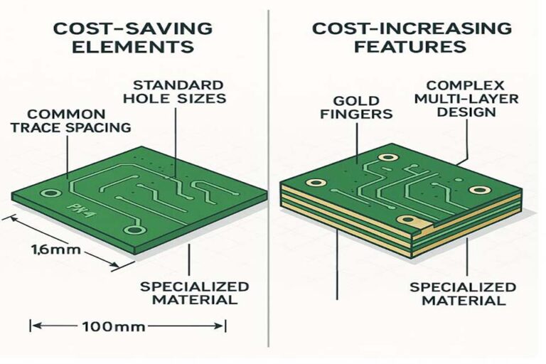
the performance of the pcb antenna is crucial. General antenna selection has a number of factors, in addition to consider the performance but also consider the cost, so in the choice of antenna, need to consider. Today we will give you various antenna design and design points.
Antennas generally have the following kinds:
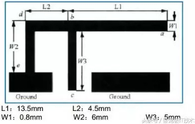
Table of Contents
What PCB antenna type ?
1.PCB antenna
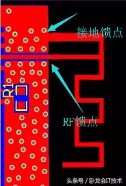
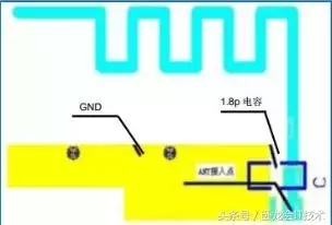
This kind of antenna cost is low, but the performance will be a little bit worse. PCB antenna also has several forms. a, planar inverted F-type antenna, the abbreviation is PIFA As shown in the figure below is the inverted F of the PCB antenna
The following is the above plane inverted F PCB antenna variant, due to the lack of space, twisted a little. Than inverted F antenna PCB design have what need to pay attention to the problem?
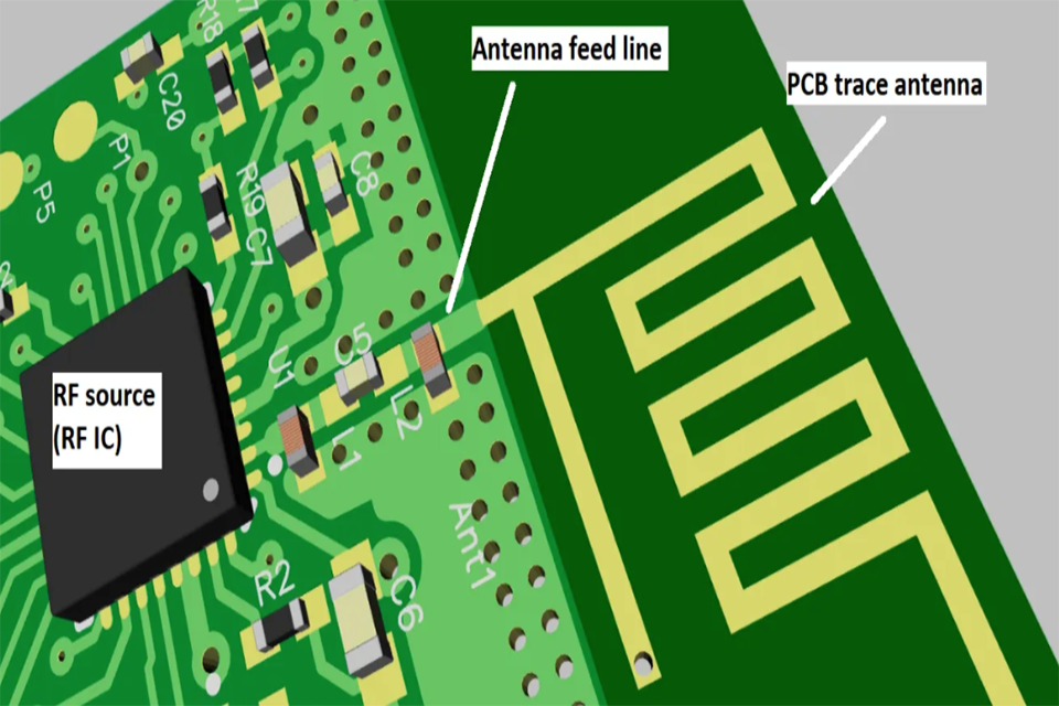
First,we need to know the RF knowledge, Shonway previously published an article, for RF, any copper foil, wire can not be seen as a simple wire, he is composed of a lot of capacitance resistance circuits an equivalent circuit, you see a short circuit, for RF is not a short circuit. With this idea we look at the PCB design of this inverted F antenna. As shown in the figure below.
six points to note about PCB antena:
- this inverted F antenna, not just draw, there are special libraries online for this antenna, take over, according to the requirements to put on it. If there is not enough space, it is their own through the simulation of their own produced their own special antenna. Original today’s headlines: Wolong will IT technology
- RF feed point here to lead out of the line impedance must be done 50ohm
- grounded feed point must be grounded securely
- the ground plane must be more to play the ground over the holes, as shown in the figure above, how much spacing is appropriate for this over the holes, if we have a previous article Wolong will be able to Bubuneng teacher wrote an article, we can find it to look at to look at
- antenna here all layers of copper foil must be net empty
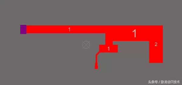
- The pcb antenna must be placed in the corner of the PCB board, it is best to three sides are empty, as shown in Figure 2, the top three sides are empty mobile phone antenna is called a planar inverted F antenna, the principle is to use a plane to connect a grounded planar feed point, and RF feed point composed of, as shown in Figure 4 below.
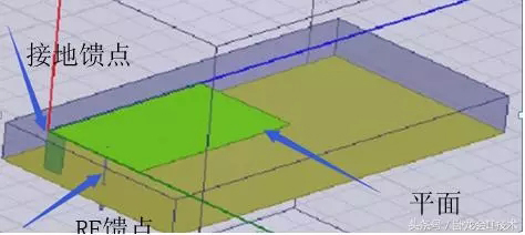
Figure 4 above from the lower left RF feed point this arrow to see the past, is an inverted. The same is the inverted F structure, but the mobile phone in the antenna using a planar structure, this inverted F antenna than the PCB board loaded antenna performance will be much better, so that the space and less, the cost is low, for the mobile phone antenna is the best choice actual antenna is shown in Figure 5 below
In fact, this plane for different mobile phones have a variety of shapes, the principle is the plane inverted F structure, in this plane one is connected to the RF, one is ground feed point is composed of the plane inverted F antenna .
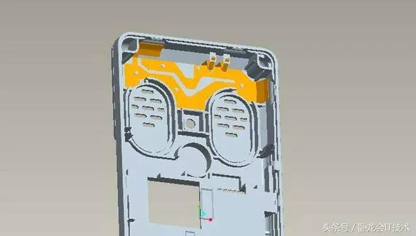
The picture above shows different mobile phone antennas. Their principles are all planar inverted F antenna, is not a long knowledge, remember to praise b, inverted L-shaped PCB board antenna
This inverted L-shaped need to pay attention to the problems with the previous almost no longer explain, inverted antenna is not inverted F-type antenna effect is a little better, because the inverted F antenna has a ground feed point, can be effectively adjusted to frequency point. There are a lot of PCB antennas on the market, mainly the above two kinds, there are some as shown in the following figure: The second kind, patch ceramic antenna.


2.patch ceramic pcb antenna

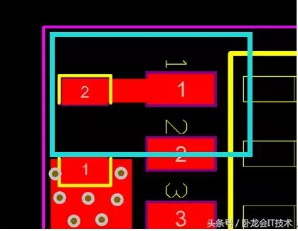
This kind of pcb antenna is made into a patch element, as shown below
One end is grounded. Ceramic antenna principle, is through an electrode called ‘antenna’ will be formed between the antenna and the ground of the high-frequency electric field into electromagnetic waves, which can This antenna is connected to one end of the RF, emitted and transmitted to the far side of the wave PCB the best layout of the wiring way is the following way

Put the ceramic patch antenna on the edge of the board, one side of the ground, one side of the RF signal, below all layers of copper foil are hollow (white box shown in the area) so that the four directions, at least two directions are empty antenna effect is very good, don’t forget to ground the copper foil should be punched on the ground over the holes, play a little more
3.Pole pcb antenna
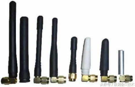
This sort of antenna is shown in Figure 14. It is one of the most effective antenna, as it is placed precede and has the best radiation performance. However, it is extra pricey and occupies more space, so it can only be exposed outside the framework.

Problems to consider when designing the PCB for this antenna
- If the RF lead is short, all layers below the RF signal line must be clear, as displayed in Figure 15. If the lead is much longer, the impedance of this lead must be regulated. For multi-layer boards, the 2nd layer listed below it should be clear, with the other layers completely copper-plated, and the reference ground need to be made use of for resistance control between layers. (Why utilize a recommendation ground between layers? Please share your opinions in the remarks section.) Insusceptibility control at 50 ohms, as received Number 16.
- The close-by grounding copper aluminum foil have to be safely grounded, which means more grounding holes must be added.
Bluetooth Antenna Layout: Upside Down F-Type Antenna: The antenna body of an upside down F-type antenna can be either linear or planar. When utilizing shielding products with a high dielectric constant, the size of the Bluetooth antenna can be lowered. As one kind of onboard antenna, the upside down F-type antenna has low layout expenses but enhances quantity somewhat. It is one of the most commonly used key in useful applications. The antenna is normally put on the top layer of the PCB, with the ground plane also on the leading layer near the antenna. Nevertheless, the area around the antenna should continue to be clear of ground aircrafts, creating an open area. As received the figure listed below:

Bluetooth Antenna Design: Rounded Antenna Design: The length of the rounded antenna is challenging to determine. The size is normally slightly longer than one-quarter wavelength, and its size is identified by its geometric geography and ground airplane. Curved-flow antennas are typically PCB-mounted, i.e., on-board antennas. Like inverted-F antennas, the antenna is typically put on the leading layer of the PCB, with the ground airplane normally situated on the top layer near the antenna. Nonetheless, the area around the antenna must not have a ground airplane; it ought to be an open room. As received Numbers 2 and 3:

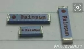
Keep in mind: Antenna length calculation formula: Antenna size (metres) = (300/f) × 0.25 × 0.96 where [stands for regularity (MHz), and 0.96 is the wavelength shortening factor. Bluetooth antenna length: roughly 300 × 12.4 GHz × 0.25 × 0.96, about 31 mm. Bluetooth antenna layout: ceramic antenna layout: Ceramic antennas are another kind of portable antenna appropriate for Bluetooth gadgets.
Ceramic antennas are categorised into block-type ceramic antennas and multilayer ceramic antennas. Since the dielectric constant of ceramic product is more than that of PCB motherboard, ceramic antennas can properly minimize antenna size. In regards to dielectric loss, ceramic materials also have lower dielectric loss than PCB circuit card, making them extremely ideal for low-power Bluetooth components. When designing the PCB, the location around the antenna must be maintained clear, with specific interest to staying clear of copper. As shown in the figure listed below:
Bluetooth Antenna Design – 2.4 GHz Pole Antenna Layout:
2.4 GHz pole Bluetooth antennas are bigger in dimension but have a more powerful transmission variety than other antennas. When creating the PCB, the location around the antenna should additionally be kept clear, comparable to the 3 antenna styles discussed over. As received the figure listed below!
Other vital considerations for Bluetooth antenna design:
- Antenna signals (frequencies over 400 MHz) are susceptible to attenuation, so the distance in between the antenna and nearby ground aircrafts need to go to the very least three times the line width.
- For microstrip lines and striplines, the particular resistance is associated with the board density, line size, vias, and the dielectric constant of the board material.
- Via holes introduce parasitical inductance, which causes significant attenuation of high-frequency signals. As a result, when directing RF traces, it is best to avoid through openings whenever feasible.