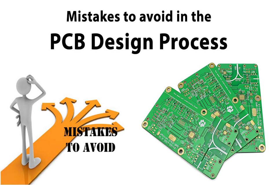
10 PCB Layout Mistakes That Result In PCB Assembly Errors
Abstract
Pcb layout flaws in published motherboard (PCBs) can considerably hinder the success of assembly and last functionality. Staying clear of essential PCB design mistakes reduces manufacturing hold-ups, reduces expenses, and makes certain high quality. This short article discovers the top 10 PCB design errors that frequently result in assembly errors, backed by design ideal practices and technological insights.
Exceptional PCB Layout exceeds simply creating a functional circuit. It includes developing for manufacturability (DFM) and assembly (DFA). A great schematic can be completely weakened by a format that is tough or difficult to construct correctly.
By staying clear of these 10 typical design mistakes, you can substantially minimize setting up errors, lower costs, and quicken your time to market.
1. Incorrect or Incomplete Component Footprints.
The Blunder:
- Using a generic footprint that doesn’t match the particular element’s datasheet, developing an impact from scratch with wrong measurements (e.g., wrong pad dimension, pitch, or spacing), or having an inaccurate pin-1 alignment.
Why It’s a Problem:
- Parts Will Not Fit: The part leads won’t line up with the pads, making automated and even manual soldering impossible.
- Poor Solder Joints: Incorrect pad sizes can cause weak solder joints, tombstoning (where a part stands up on one end), or solder connecting.
- Circuit Failing: If the pin mapping is wrong, the circuit will not operate and elements might be harmed.
Exactly how to Repair It:
- Trust fund the Datasheet: Constantly use the maker’s datasheet for the specific part number you are making use of. It will certainly include a “Recommended Land Pattern.”.
- Make Use Of IPC-Compliant Footprint Generators: A lot of modern EDA (Electronic Style Automation) software consists of tools to generate IPC-7351 compliant footprints based on element measurements.
- Confirm Pin 1: Double-check that the pin-1 indicator on your footprint matches the indicator on the physical element.
2. Insufficient Component-to-Component Clearance.
The Error
Positioning elements as well near to each other is a classic DFA error.
- Securely loading elements without thinking about the physical requirements of the setting up process.
Why It’s a Problem:
- Pick-and-Place Collisions: The nozzle of the pick-and-place device may ram a surrounding, taller element when placing a smaller one.
- Soldering Problems: Solder connecting can easily occur in between the pads of surrounding parts throughout reflow soldering.
- Rework is Difficult: If an element stops working, there is no physical space for a technician to use a hot air device or blowpipe to eliminate and replace it without harming its next-door neighbors.
Exactly how to Repair It:
- Define DRC Policies: Establish Design Regulation Checks (DRC) in your software program for component-to-component spacing. A general guideline is to leave at the very least 0.5 mm (20 mils) in between smaller sized components and even more for bigger or taller ones.
- Consult Your Assembler: Your contract manufacturer (CENTIMETERS) can give you with their certain clearance requirements based upon their devices.
3. Overlooking Thermal Alleviations.
The Blunder:
Huge copper puts and ground planes are excellent for thermal administration and signal stability, yet they can be a nightmare for soldering.
- Connecting an element pad directly to a big copper aircraft without a thermal alleviation.
Why It’s a Problem:
- The copper aircraft functions as an enormous warm sink, wicking warmth away from the pad during soldering. This prevents the pad from getting to the correct reflow temperature level, leading to a chilly solder joint . This is a covert problem that can pass first screening but stop working later on in the area.
Exactly how to Repair It:
- Use Thermal Reliefs: In your EDA software program, make sure that pads attaching to large copper airplanes make use of a thermal relief pattern (commonly resembling spokes on a wheel). This creates a thermal bridge, allowing the pad to warm up adequately while still maintaining a solid electrical connection to the aircraft.
4. Silkscreen Over Pads.
The Mistake:
Silkscreen is the ink layer made use of for component designators, logos, and other markings. While valuable, it can cause serious issues if lost.
- Placing silkscreen text or lines in addition to revealed copper pads where elements will certainly be soldered.
Why It’s a Problem:
- The ink avoids solder from correctly wetting the pad. This produces an undependable or non-existent solder joint, causing an open circuit. Throughout setting up, the part may be skewed or gravestone as it tries to pick an irregular surface.
Exactly how to Repair It:
- Run a DRC Inspect: Your EDA software has a details check for silkscreen-to-pad clearance. Run it and take care of all offenses.
- Keep Clearance: Ensure there is a minimal clearance (e.g., 0.1 mm or 4 mils ) between any type of silkscreen aspect and the side of a solder pad.
5. Via-in-Pad (Without Appropriate Handling).
The Mistake:
Positioning a by means of straight in the facility of a surface-mount pad is a fantastic way to save area, yet it needs an unique manufacturing action.
- Designing with vias directly in the solder pads without specifying to the maker that they need to be plugged and plated over .
Why It’s a Trouble:
- During reflow soldering, the molten solder will be evil down right into the by means of barrel by capillary action. This starves the pad of solder, leading to an inadequate or open solder joint. This is especially bothersome for BGA (Round Grid Range) elements.
Exactly how to Repair It:
- Best Practice: The best remedy is to move the using simply outside the pad and attach it with a brief trace (known as “dog-bone” design).
- If You Should Use Via-in-Pad: Clearly specify in your fabrication notes that vias in pads need to be ” connected and plated over” (or “filled and topped”). This is an added process step with a connected cost, but it’s important for a dependable setting up.
6. Missing or Poorly Put Fiducial Markers.
The Error:
Fiducials are small copper pens on the PCB that function as recommendation points for automated optical devices, like pick-and-place machines.
- Neglecting to add fiducials to the layout, or putting them in non-optimal locations.
Why It’s an Issue:
- Without clear fiducials, the pick-and-place device can not accurately “see” the board’s placement and orientation. This results in organized part positioning errors, where all parts are shifted or revolved, assuring a stopped working setting up.
Exactly how to Repair It:
- Make Use Of Panel Fiducials: Place at least 3 fiducials on the PCB, ideally in an “L” form near the corners.
- Utilize Local Fiducials: For fine-pitch elements like BGAs or QFPs, area 1 or 2 neighborhood fiducials near the element for higher-precision positioning.
- Standard Layout: A regular fiducial is a 1mm diameter copper circle with a 2mm size solder mask clearance. Do not cover it with silkscreen.
7. Incomplete or Uncertain Production Documents.
The Error:
The layout files you send out to your assembler are their only user’s manual. Any kind of ambiguity will certainly cause hold-ups or mistakes.
- Supplying a Bill of Products (BOM) with missing out on Supplier Part Numbers (MPNs), an insufficient Centroid (Pick-and-Place) file, or uncertain assembly notes.
Why It’s an Issue:
- Incorrect Parts Ordered: Without a certain MPN, the assembler may purchase a part with the same value however a different package, voltage ranking, or resistance.
- Part Placement Errors: An incorrect Centroid data will certainly create parts to be placed in the incorrect location or with the incorrect turning.
- Production Stops: The assembler will certainly have to quit production and call you for information, delaying your project.
Exactly how to Repair It:
- Develop a Perfect BOM: Consist of referral designators (R1, C1, U1), amount, value, a specific MPN, bundle kind (0402, SOIC-8), and a “Do Not Set Up” (DNI) column if required.
- Verify Your Centroid Documents: Guarantee it consists of the recommendation designator, X-Y collaborates, turning, and board side (Top/Bottom) for each component.
- Offer Clear Assembly Illustrations: Make use of illustrations to highlight unique guidelines, polarization (for diodes, caps), and any manual assembly steps.
8. Neglecting Panelization Policies.
The Mistake:
For volume manufacturing, boards are not constructed one by one. They are organized right into a bigger “panel.”.
- Positioning parts too near to the edge of the board, without considering how the boards will certainly be separated from the panel.
Why It’s an Issue:
- Elements near the side can be damaged by the router or v-groove scoring tool used for depaneling. There may additionally want clearance for the tooling rails that hold the panel in the assembly makers.
Exactly how to Repair It:
- Maintain Edge Clearance: Maintain all elements a minimum of 2.5 mm (100 mils) away from the board side, particularly if using v-grooves.
- Review with Your CM: Talk with your setting up home regarding their chosen panelization technique (v-groove vs. tab-routing with “mouse attacks”) and layout as necessary.
9. Poor Solder Mask Layout
The Blunder:
The solder mask is the safety layer that stops solder from shorting surrounding traces. An improperly defined mask is as bad as no mask whatsoever.
- Developing solder mask “dams” or “slivers” (the mask between pads) that are also slim.
Why It’s a Problem:
- If the solder mask internet between 2 fine-pitch pads is below the fabricator’s minimum capability (e.g., < 3 mils), it will certainly not adhere effectively. It can exfoliate throughout production or soldering, fall onto a pad, and cause a solder bridge (brief circuit).
Exactly how to Repair It:
- Know Your Fab’s Specs: Inspect your fabricator’s minimum solder mask web/sliver width and establish this generally in your DRC.
- Use Gang Covering Up for Fine-Pitch: For exceptionally fine-pitch components where a trustworthy dam is difficult, it’s much better to have the fabricator make use of a single “ganged” solder mask opening for a row of pins.
10. Poor Element Option & Lifecycle Administration.
The Error:
A style can be perfect for assembly yet difficult to construct because the parts aren’t available.
- Creating with components that are rare, Not Suggested for New Designs (NRND), or at End-of-Life (EOL). Also, choosing incredibly tiny bundles (like 01005) when not absolutely essential.
Why It’s a Trouble:
- Supply Chain Delays: If an important part has a 52-week lead time or runs out stock anywhere, your project is dead in the water.
- Greater Assembly Costs: Ultra-small or exotic packages call for advanced equipment and stricter procedure control, boosting assembly costs.
Exactly how to Repair It:
- Examine Supply Throughout Layout: Use vendor sites (e.g., Digi-Key, Mouser, Octopart) to inspect supply levels and preparation while you are making .
- Prevent EOL/NRND Components: The majority of vendor web sites will certainly flag components that are not advised for brand-new layouts. Follow these warnings.
- Specify Alternatives: In your BOM, give 1 or 2 pre-vetted alternate component numbers for usual parts like resistors and capacitors.
FAQs
What is the most common source of PCB setting up failing?
One of the most typical causes are wrong part footprints and lack of DFM checks, which result in misaligned parts and soldering flaws.
Why is via-in-pad a trouble in PCB assembly?
Via-in-pad can wick solder far from the pad, resulting in weak joints or opens up unless filled up and plated effectively.
Exactly how can I ensure my PCB layout is assembly-ready?
Job closely with your PCB assembly producer during design, run DFM checks, and comply with IPC criteria.
Are fiducials constantly called for on a PCB?
Yes, especially for automated assembly. Worldwide fiducials help overall board positioning, while neighborhood fiducials are needed for fine-pitch components.
Verdict
Staying clear of these 10 usual style blunders drastically enhances the success price of PCB setting up. A properly designed board ensures smooth shift from prototype to manufacturing, decreases setting up mistakes, and minimizes price overruns. Cooperation with your PCB setting up producer throughout the layout stage is essential.