-
Xinxintian Industrial Zone, Shajing Street,Bao'an District, Shenzhen, China

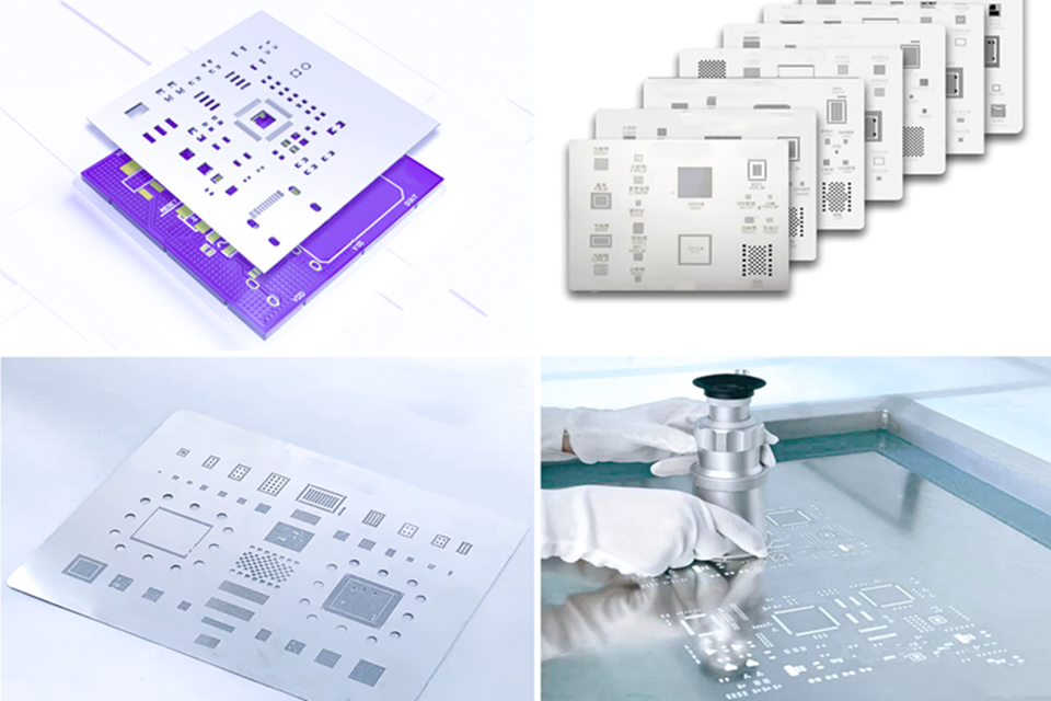
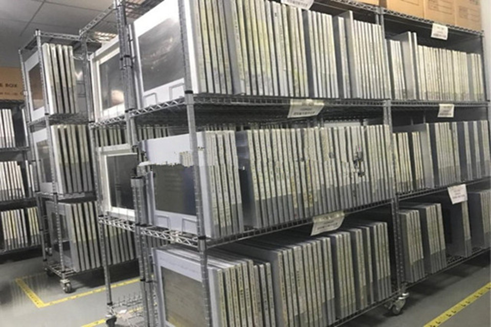
Stencil
What is PCB Stencil?
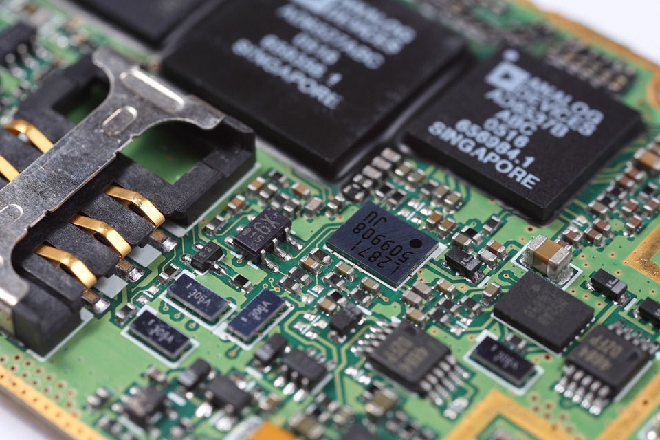
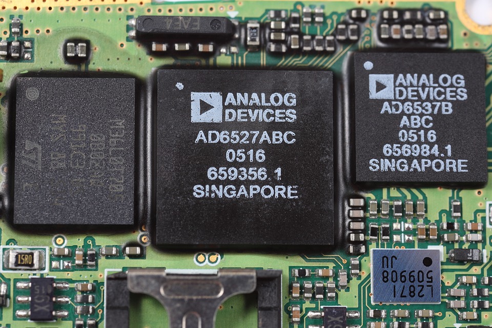
In the field of electronics manufacturing, PCB component installation is mainly divided into Plug-in, SMT (Surface Mount Technology) and Mixed Assembly three ways. Among them, SMT assembly and hybrid assembly highly dependent on a key tool – Stencil (SMT Stencil), which is not only Smoke Paste Printing precision moulds, but also to ensure that the quality of the circuit board is the core components.
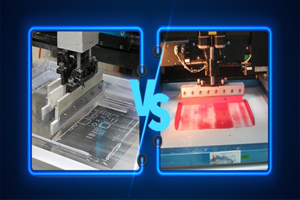
The SMT Stencil is a mesh mould made of a high-precision metal (e.g. stainless steel or alloy), whose core function is the precise deposition of paste. By aligning with the PCB board, the stencil transfers the pre-designed opening pattern to the board surface, ensuring that the paste volume and positional accuracy are controlled at the micron level, thus providing a solid soldering foundation for subsequent component placement. This process directly affects the board soldering quality, component positioning accuracy and product yield, is SMT process in the irreplaceable key links.
Why stencil is ‘hidden champions’ among SMT Technology ?
- Precision determines success or failure: The stencil’s opening size, thickness (e.g. 0.1mm-0.3mm) and edge finish directly determines the paste’s uniformity and positional accuracy, especially in high-density PCBs or micro-components (e.g. 0201 packages) assemblies.
- Enhancement of productivity: High quality stencils can reduce Solder Bridge, Less Tin/More Tin Defects, reduce Rework, and speed up Mass Production.
- Cost Optimisation: Long-lasting stencils (e.g. Laser Cut Stencils or Electroformed Stencils) can be reused hundreds of times, significantly reducing Veneer Processing Costs.
What the criterion for SMT stencil ?
- Application Scenario Matching: Select conventional stencils, multilayer stencils or red glue printing solutions according to the PCB design (e.g., complex components such as QFN, BGA, etc.).
- Process adaptability: Optimise stencil opening shape (trapezoidal/tapered) and thickness in combination with paste type (lead/lead-free), printer model and reflow process.
- Vendor Technical Strength: Prefer vendors with micron-level machining accuracy and 3D profile inspection capabilities to ensure that stencil customisation requirements (such as ultra-fine line or blind hole adaptation) are accurately achieved.
What are types of SMT stencil and How to Choose correct Stencil ?
Stencil Types and Selection Guide
Comparison of 7 types of stencils
| Type | Advantages (✅) | Disadvantages (❌) | Applicable scenarios |
|---|---|---|---|
| Laser stencil | ✅ High precision (±4μm) ✅ Trapezoidal hole wall helps solder paste release | ❌ High cost ❌ Poor applicability for fine pitch | SMT solder paste printing, precision electronic components |
| Electropolished stencil | ✅ Ultra-smooth hole wall (<3μm) ✅ Corrosion resistant | ❌ High cost of secondary processing ❌ Complex process | High-precision solder paste printing, chip packaging |
| Electroforming stencil | ✅ Ultra-fine pitch (0.3mm+) ✅ Excellent hole wall sealing | ❌ Complex process ❌ Expensive cost | BGA/QFP components, microelectronics manufacturing |
| Step steel mesh | ✅ Precise control of solder paste amount ✅ Multi-thickness adaptation | ❌ Fast scraper wear ❌ Complex design | Complex PCB printing, high-density components |
| Bonding steel mesh | ✅ Micro aperture (0.1mm level) ✅ High-precision positioning | ❌ Extremely high cost ❌ High process threshold | Wafer-level packaging, chip bonding |
| Nickel-plated steel mesh | ✅ Ultra-smooth hole wall (0.4μm) ✅ Long life | ❌ Difficult to control plating uniformity ❌ High cost | High life demand scenario, precision equipment |
| Etched steel mesh | ✅ Low cost ✅ Fast batch production | ❌ Low precision ❌ Rough hole wall | General printing, low precision demand |
3 main points in choosing a stencil
Precision is given priority :
- Electrophormed Stencil (Ultra-Fine Pitch) or Bonded Stencil (Tiny Aperture)
- scenario : 0201 component printing, high density PCB
Cost Control :
- Laser Stencil (Balance accuracy and cost) or Etched stencil (low cost general objective)
- scenario : Mass Production Stencil, SMT Solder Paste Printing
Special Requirements :
– Nickel-plated stencils (corrosion-resistant + long life) or Step STNIL (Complex PCB Adaptation)- scenario : precise equipment stencil, multilateral board printing
Why US to be your SMT stencil Partner in China ?

- 13 years of industry experience: Focus on precision stencil processing, covering consumer electronics, industrial control, automotive electronics and other fields, to meet the demand of small batch trial production to million level mass production.
- Full process chain support: Provide CAD data conversion, stencil design optimisation, laser/electroforming processing and gold/nickel plating enhancement services to extend the life of the stencil.
- Rapid Response: 48-hour sample delivery, support for urgent orders and global logistics, helping customers seize market opportunities.