-
Xinxintian Industrial Zone, Shajing Street,Bao'an District, Shenzhen, China
Designing for Success: Top Tips for Effective PCB Layout
[ad_1]
Designing for Success: Top Tips for Effective PCB Layout
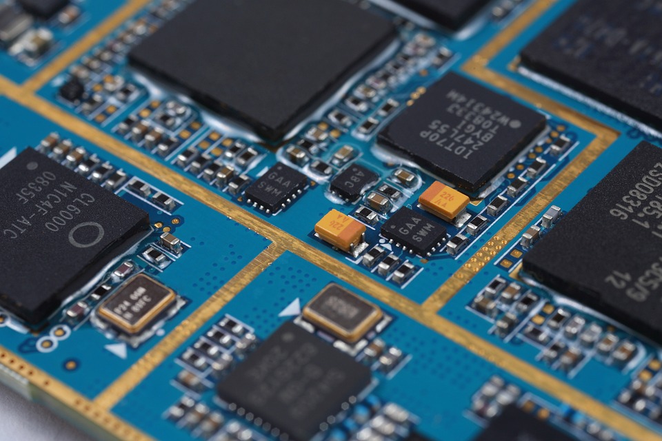
The Printed Circuit Board (PCB) is a critical component in the production of electronic devices. Its design and layout have a significant impact on the overall performance and durability of the final product. In this article, we will provide you with top tips for designing an effective PCB layout to ensure successful production.
### 1. Plan Your Design
Before starting the design process, it is essential to have a clear understanding of what you want to achieve with your PCB. Define the project requirements, identify the components and positions them on the board. Consider the size and shape of the components, the wiring and power distribution, and the layout of the circuitry. Plan your design carefully to ensure that it can accommodate the components and cables without any clashes or misalignments.
### 2. Use a Symbolic Representation
Use a symbolic representation of the components on the PCB layout to simplify the design process. Symbols are used to identify the components, and can be easily moved, copied, or deleted. This approach helps to reduce the complexity of the design and improve its readability.
### 3. Focus on Component Placement
The placement of components on the PCB is crucial for effective design. Consider the properties of each component, such as its size, shape, and position, when placing it on the board. Ensure that the components are placed in a way that they can be easily connected and accessed. Overcrowding can lead to design errors, and poor component placement can cause the board to be unreadable.
### 4. Use a Grid to Measure Distances
To ensure accurate and efficient component placement, use a grid system to measure distances. This will help to prevent errors in the placement of components and ensure that they are properly aligned. A grid system can also be used to measure the distance between components and connect them correctly.
### 5. Check Component Orientation
Orientation is important when placing components on the PCB. Check the orientation of each component and ensure that it is correct. Improper orientation can cause design errors and affect the performance of the final product.
### 6. Optimize Component Placement
Optimize component placement to reduce waste space and improve component density. Proper component placement can help to reduce the size of the board and improve its overall performance. Consider the size and shape of each component, as well as the connections required, to place them in a way that optimizes the design.
### 7. Consider Component Modeling
Component modeling is a technique used to enhance the accuracy of the PCB design. This approach involves creating a virtual model of the components and simulating their behavior on the board. This can help to identify potential design errors, such as component clashes, and ensure that the design is accurate before sending it to the manufacturer.
### 8. Use Industry Standards
Industry standards and guidelines are essential for ensuring that the PCB design meets the required specifications and regulations. Familiarize yourself with industry standards and guidelines to ensure that your design meets the necessary requirements.
### 9. Check for Errors
Check the design for errors and inconsistencies, including component clashes, misaligned pins, and inconsistent spacing. Errors can be critical and affect the performance of the final product. Regularly check the design to ensure that it is error-free and meets the required specifications.
### 10. Document Your Design
Document your design to ensure that it is easy to understand and maintain. Document the design parameters, component specifications, and layout details. This will help to simplify the design process and improve the efficiency of the manufacturing process.
### Conclusion
Designing an effective PCB layout requires careful planning, attention to detail, and a focus on component placement, orientation, and modeling. By following these top tips, you can ensure that your design is accurate, efficient, and meets the required specifications. Remember to plan your design, use a symbolic representation, focus on component placement, use a grid to measure distances, check component orientation, optimize component placement, consider component modeling, use industry standards, check for errors, and document your design.
### FAQs
* How do I start designing a PCB layout?
To start designing a PCB layout, begin by defining the project requirements and identifying the components needed. Use a symbolic representation to create a plan for the design, and then place the components on the board carefully.
* What is the best way to place components on a PCB?
The best way to place components on a PCB is to use a grid system to measure distances, and to consider the properties of each component, such as its size, shape, and position.
* How do I check for errors in my PCB design?
To check for errors in your PCB design, regularly review the design for component clashes, misaligned pins, and inconsistent spacing. Use industry standards and guidelines to ensure that the design meets the required specifications.
* What is component modeling, and why is it important?
Component modeling is a technique used to enhance the accuracy of the PCB design by creating a virtual model of the components and simulating their behavior on the board. This can help to identify potential design errors and ensure that the design is accurate before sending it to the manufacturer.
* What are some common mistakes to avoid when designing a PCB?
Some common mistakes to avoid when designing a PCB include failing to consider component orientation, not using a grid system, and not checking the design for errors.
[ad_2]

admin
You may also like

The Benefits of Routing Optimization: How ICfabrication Can Streamline Your PCB Design Process
High-Speed PCB Design: Techniques and Considerations for Fast and Reliable PCBs – Strategies for designing PCBs that can handle increased signal speeds and data transfer rates.

PCB Assembly for IoT and Wearable Devices: The Rise of Miniaturization