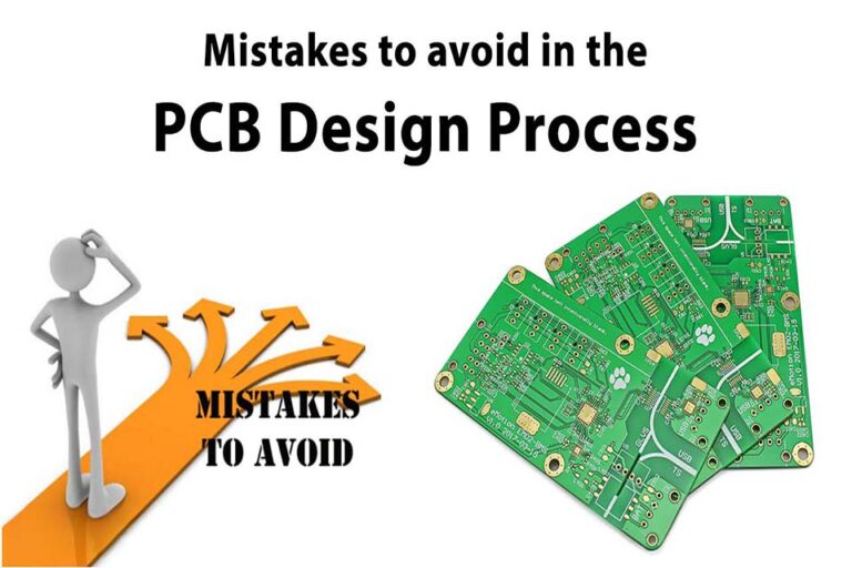
حل مشكلة اختبار لوحة الدوائر المطبوعة: تحليل كامل لست مشكلات وحلول شائعة
خلاصة
In the field of electronic manufacturing, the testing of printed circuit boards (PCBs) is directly related to product quality and delivery efficiency. This article systematically analyzes the core value of PCB testing, six common problems and targeted solutions, and provides practical guidance for engineers and purchasing managers through authoritative data and industry cases. The article covers key links such as test strategy formulation, test point design optimization، و test equipment selection, helping companies achieve full-process quality control from design to mass production.
جدول المحتويات
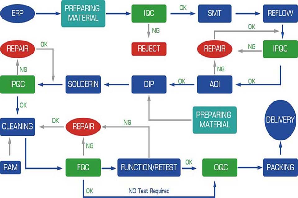
1. The core value of PCB testing: dual guarantee of quality and efficiency
1.1 Testing is the “physical examination center” of electronic products
Whether it is a smart watch for consumer electronics or a navigation system for aerospace, PCB testing is like the “physical examination center” of the product. According to statistics from IPC (International Electronics Industry Association), more than 70% of circuit failures can be traced back to the assembly stage, and scientific testing can reduce the product rework rate by more than 40%.
1.2 The triple defense network of the test process
- Optical inspection (AOI): Capture 0.01mm level defects through high-precision cameras ([Illustration suggestion: insert the working principle diagram of AOI inspection equipment])
- X-ray inspection (AXI): Penetration scanning of hidden solder joints
- Functional test (FCT): Simulate real working conditions to verify circuit performance
1.3 The art of balancing test costs and benefits
Industry data shows that every $1 invested in the test stage can avoid $10 in later rework costs. However, excessive testing will extend the delivery cycle, and the test combination needs to be selected according to product complexity and output
2. Six major PCB testing problems and solutions
2.1 Problem 1: Lack of test strategy – invisible trap in the design stage
Core pain point: 85% of test failures are due to the failure to reserve test space in the design stage
حل:
- DFT (Design for Testability) Golden Rule:
- Design accessible test points for each network
- يستخدم standardized test point spacing (recommended ≥50mil)
- Reserve debugging stub position (recommended diameter ≥100mil)
- Case reference: A drone company increased the test coverage from 65% to 98% through DFT optimization

2.2 Problem 2: Insufficient test point coverage – “blind spot crisis” of circuit boards
Fatal impact: Hidden networks may cause intermittent short circuits, causing the product to suddenly fail after 3 months of use
Cracking strategy:
- Three principles of test point design:
- At least 1 test point for each signal network
- Set redundant test points for key power/ground networks
- Ensure electrical continuity when using vias to replace test points
- Tool recommendation: Automatic test point annotation function of Altium Designer2.3 Problem 3: Insufficient test point spacing – the physical bottleneck of automated testingTypical consequences: Probe interference causes test misjudgment rate to increase by 20%Optimization solution:
| Area type | Recommended spacing (mil) | Remarks |
|---|---|---|
| Test point and component | ≥50 | It is recommended to use isolation zone design |
| Test point and edge | ≥100 | Reserve test fixture installation area |
| Between test points | ≥30 | Fan-out wiring can be used in high-density areas |
2.4 Problem 4: Manual testing is not accessible – nightmare of on-site debugging
Industry pain point: 73% of maintenance engineers reported that blind testing takes up 40% of the total maintenance time
حل:
- Design improvement:
- Mark Network name (such as VCC_3V3) on the silk screen layer
- يستخدم Color coding system to distinguish test areas
- Reserve Test jumper holes (recommended size 2.0mm)
- Tool assistance: Oscilloscope probe adapter set
2.5 Problem 5: Test fixture version confusion – fatal hidden danger in mass production stage
Cost warning: Production line downtime loss caused by wrong fixtures can reach $50,000/hour
Management strategy:
- Fixture life cycle management:
- Establish Version control database (GitLab is recommended)
- Implement Change Impact Analysis (CIA) process
- يستخدم Modular fixture design to reduce transformation costs
- Alternative solution: Flying probe tester (recommended JUKI FX-3 series)
2.6 Question 6: Compatibility trap of obsolete components – the invisible killer of technology iteration
Risk data: Circuit boards using discontinued components have a test failure rate 3.2 times higher than new components
Alternative strategy:
- Component library management:
- Establish supplier life cycle tracking system
- Adopt parametric alternative solutions (such as replacing 7812 with 12V LDO)
- Utilize ECAD tool BOM warning function
- Industry resources: TI’s device replacement calculator
3. FAQ: Seven high-frequency problems of PCB testing
How to choose a suitable PCB test method?
Decision based on the following matrix:
Test type
السيناريوهات القابلة للتطبيق
المزايا
العيوب
تكنولوجيا المعلومات والاتصالات
Medium and large-volume production
Fast speed (<10s/board)
High fixture cost
مقاطعة العاصمة الفيدرالية
Functional verification
Simulate real working conditions
Complex test program development
هيئة الاستثمار العربية
Surface defect detection
No contact required
Unable to detect internal defects
AXI
Hidden solder joint detection such as BGA
High accuracy (μm level)
Large equipment investment
What are the best practices for test point design?
Follow the IPC-J-STD-020 standard and adopt the ring test point design to ensure:
Diameter ≥15mil
Copper thickness ≥1oz
Electrically isolated from the main pad
How to evaluate test coverage?
Using Boundary Scan Test (JTAG) with TestPoint software, you can generate:
Network coverage heat map
Fault location probability analysis
Test time optimization suggestions
How to control the test cost of small batch production?
أ: Adopt hybrid test strategy:
Prototype stage: يستخدم Handheld multimeter + oscilloscope (Keysight U1272A** recommended)
Trial production stage: Deploy Flying probe tester (SCHMIDT FPT-3000** recommended)
Mass production stage: Customize Special test fixture
How to deal with the test fixture update problem?
أ: ينفذ fixture change management process:
Evaluate the impact level of design changes (level 1-5)
For changes ≤ level 3, use modular fixture transformation
For changes ≥ level 4, start flying probe test transition plan
How to ensure the traceability of test data?
Deploy MES system (recommended Siemens SIMATIC IT), to achieve:
Cloud storage of test data
Trace defective products to specific work orders
Automatic generation of ISO9001 compliance reports
4. Summary: Build a golden triangle system for PCB testing
Today, with the increasingly fierce competition in the electronics manufacturing industry, PCB testing has evolved from simple quality inspection to system engineering practice. Through prevention on the design side, precision on the test side and cooperation of the supply chain, enterprises can build a complete quality protection system. It is recommended to adopt DFM+DFT joint design mode (, in conjunction with annual test capability audit, to continuously optimize the test process.