-
Xinxintian Industrial Zone, Shajing Street,Bao'an District, Shenzhen, China
PCB Manufacturing 101: A Beginner’s Guide to Printed Circuit Board Production – A comprehensive overview of the PCB manufacturing process, from design to production.
[ad_1]
PCB Manufacturing 101: A Beginner’s Guide to Printed Circuit Board Production
Introduction
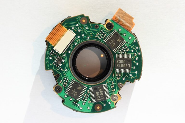
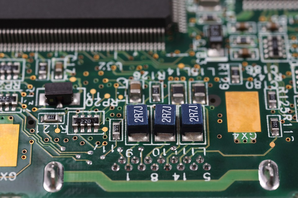
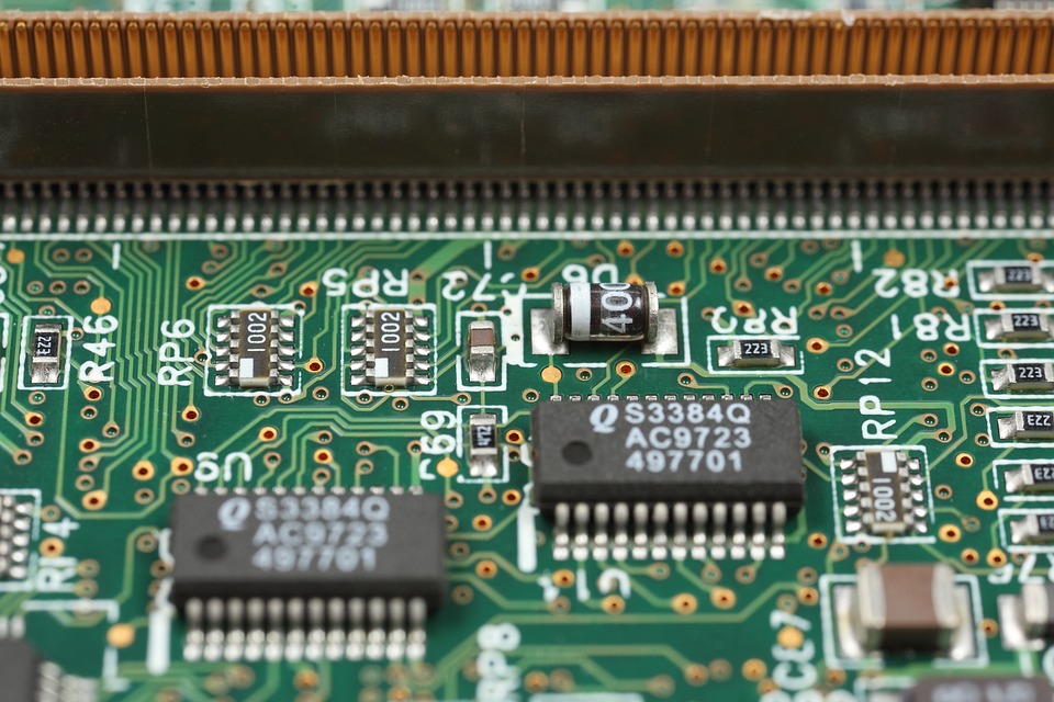
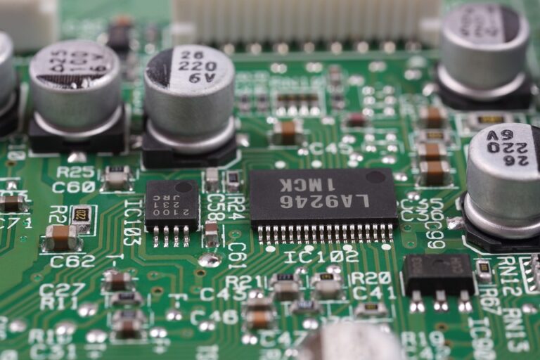
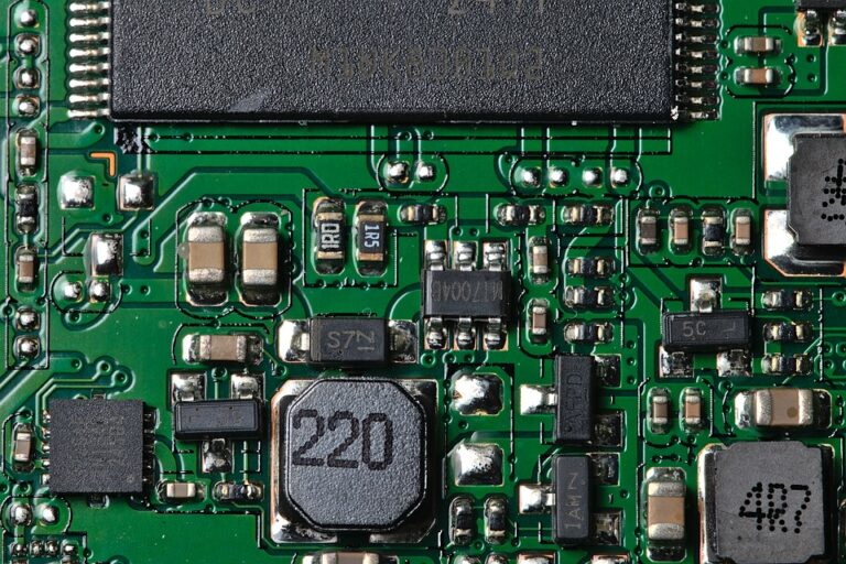
Printed Circuit Boards (PCBs) are the backbone of modern electronics. They serve as the foundation for a wide range of devices, from smartphones to computers, medical equipment, and more. PCB manufacturing is a complex process that involves multiple stages, from design to production. In this article, we’ll take you on a journey through the PCB manufacturing process, exploring the different steps involved, and providing an overview of the latest technologies and techniques used in modern PCB production.
Design Stage
The first stage of PCB manufacturing is the design stage. This is where engineers and designers use specialized software to create a detailed design of the PCB, taking into account the components, their placement, and the necessary copper tracks. The design must also consider factors such as heat dissipation, electrical integrity, and manufacturing limitations.
The design stage typically involves several steps:
*
- Schematic design: Engineers create a diagram of the electronic circuit, identifying the components, their values, and their interconnections.
- Layout design: The schematic design is then converted into a two-dimensional layout, which includes the physical placement of components and the copper tracks.
- Signal integrity analysis: The design is analyzed to ensure that it meets the required signal integrity standards.
- Manufacturing rule checks: The design is checked against manufacturing rules to ensure that it can be produced without issues.
*
*
*
Mask Creation
Once the design is complete, it’s time to create the mask. The mask is a photographic image that defines the copper tracks and other features on the PCB. There are two types of masks: the photomask and the wet mask.
The photomask is used for photolithography, a process that transfers the design onto the PCB. The photomask is a clear plastic film coated with a thin layer of silver or other metal. The design is etched onto the photomask, and it’s then used to expose the PCB to ultraviolet light.
The wet mask is used for etching and is a thin layer of photoresist applied to the PCB. The design is printed onto the wet mask using inkjet or other printing technology. The wet mask is then immersed in a solvent, which etches away the unwanted areas, leaving the design intact.
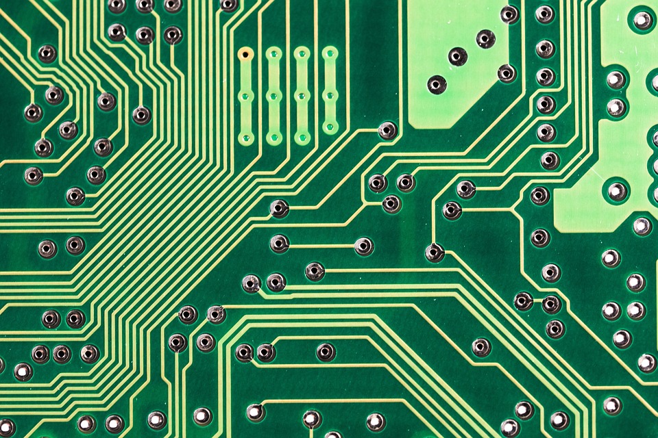
Copper Cladding
The next step is the copper cladding process. This involves applying a layer of copper foil to the substrate, which is typically made of FR4 (a type of fiberglass-reinforced epoxy resin). The copper foil is carefully cut to the correct size and shape to ensure a precise fit.
The copper cladding process involves several steps:
*
- Copper foil cutting: The copper foil is cut to the correct size and shape.
- Copper foil application: The copper foil is applied to the substrate, ensuring a smooth and even layer.
- Copper etching: The copper foil is etched using a chemical process to create the desired design.
- Copper surface finish: The copper surface is cleaned and coated with a layer of solder mask and silkscreen.
*
*
*
Laminating
Laminating involves bonding the copper foil to the substrate using a combination of heat and pressure. This process creates a strong bond between the copper foil and the substrate, ensuring that the PCB is robust and reliable.
There are two types of lamination: autoclave and hot press. Autoclave laminating uses a combination of heat and steam to bond the materials, while hot press laminating uses heat and pressure alone.
Dry Film Lamination
Dry film lamination is a process that uses a dry film photoresist to create the desired design. This process is similar to wet mask etching but uses a dry film instead.
The dry film is applied to the copper foil, and then the PCB is exposed to ultraviolet light, which causes the photoresist to harden. The excess photoresist is then removed, leaving the desired design.
Epoxy Coating
Epoxy coating is a process that applies a layer of epoxy resin to the PCB to provide additional protection and insulation. This process is often used to encapsulate components, such as SMDs (Surface Mount Devices), to prevent damage or contamination.
Solder Mask and Silkscreen
Solder mask and silkscreen are two additional processes that enhance the functionality and appearance of the PCB.
Solder mask is a layer of insulating material applied to the copper tracks, preventing accidental short circuits during the soldering process. Silkscreen is a layer of conductive ink used to print labels, logos, and other graphics onto the PCB.
Finishing
The final stage of PCB manufacturing is finishing. This involves a range of processes, including:
*
- Copper polishing: The copper surface is polished to ensure a smooth finish.
- Board cutting: The PCB is cut to the correct size using a die-cutting process.
- Panelization: Multiple PCBs are cut from a single panel using a CNC cutting machine.
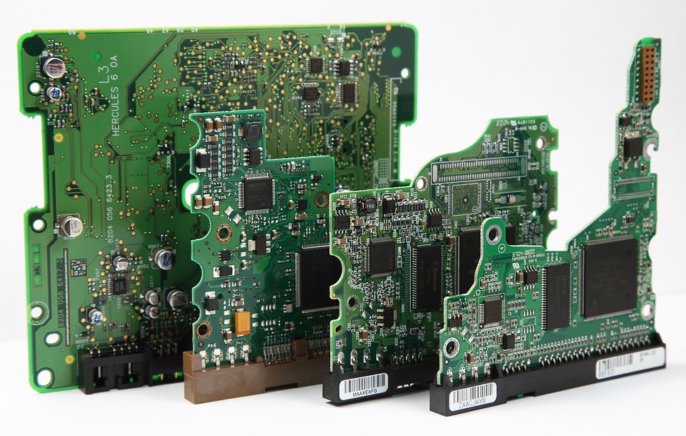
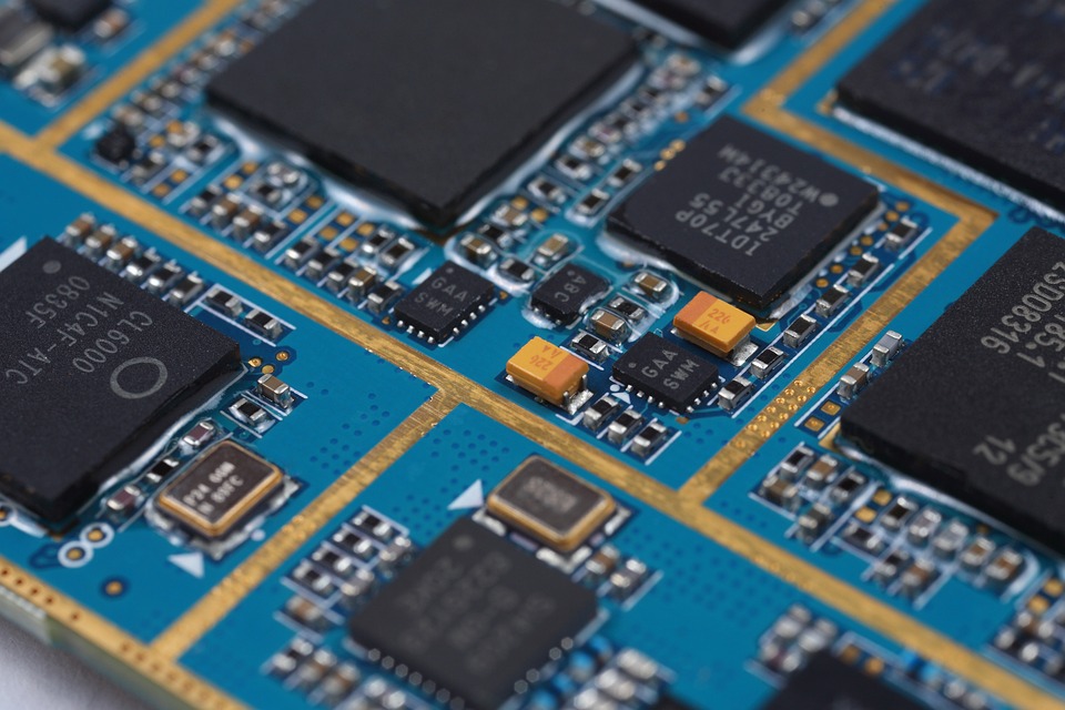
- Assembly: The PCB is assembled by attaching components using surface mount technology (SMT) or through-hole technology (THT).
*
*
*
Conclusion
PCB manufacturing is a complex process that requires precision, accuracy, and attention to detail. From design to production, the process involves multiple stages, each with its own set of challenges and considerations.
In this article, we’ve provided an overview of the PCB manufacturing process, highlighting the different stages and techniques used in modern PCB production. Whether you’re a beginner or an experienced professional, understanding the PCB manufacturing process is essential for designing and building reliable and high-quality electronic devices.
FAQs
- What is the purpose of the photomask in PCB manufacturing?
- The photomask is used to transfer the design onto the PCB during the photolithography process.
- What is the difference between photomask and wet mask etching?
- Photomask etching uses a clear plastic film coated with metal to create the design, while wet mask etching uses a layer of photoresist applied to the PCB.
- What is the purpose of solder mask and silkscreen?
- Solder mask prevents accidental short circuits during the soldering process, while silkscreen is used to print labels, logos, and other graphics onto the PCB.
- What is the purpose of laminating in PCB manufacturing?
- Laminating involves bonding the copper foil to the substrate using heat and pressure, creating a strong bond between the materials.
[ad_2]

admin
You may also like
The Evolution of PCB Technology: A Look at the Latest Advancements
The Benefits of SMT vs. Through-Hole Mounting: Which is Right for Your PCB?

The Benefits of Routing Optimization: How ICfabrication Can Streamline Your PCB Design Process