25 de sfaturi de proiectare PCB pentru economisirea costurilor pentru fabricarea și asamblarea PCB-urilor
pcb design is important for the production ,Designing for cost-effectiveness is a critical ability for any type of hardware engineer. Financial savings in the layout phase have a substantial downstream effect on both manufacturing (construction) and setting up expenses, specifically at scale.
Right here are 25 cost-saving PCB layout pointers, broken down into 3 essential areas: Board Fabrication (DFM) , Part & Assembly (DFA) și Refine & Logistics .
Cuprins
Part A: Board Construction (Design for Manufacturability – DFM)
These suggestions focus on the raw PCB itself, before any kind of components are placed.
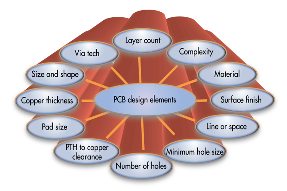
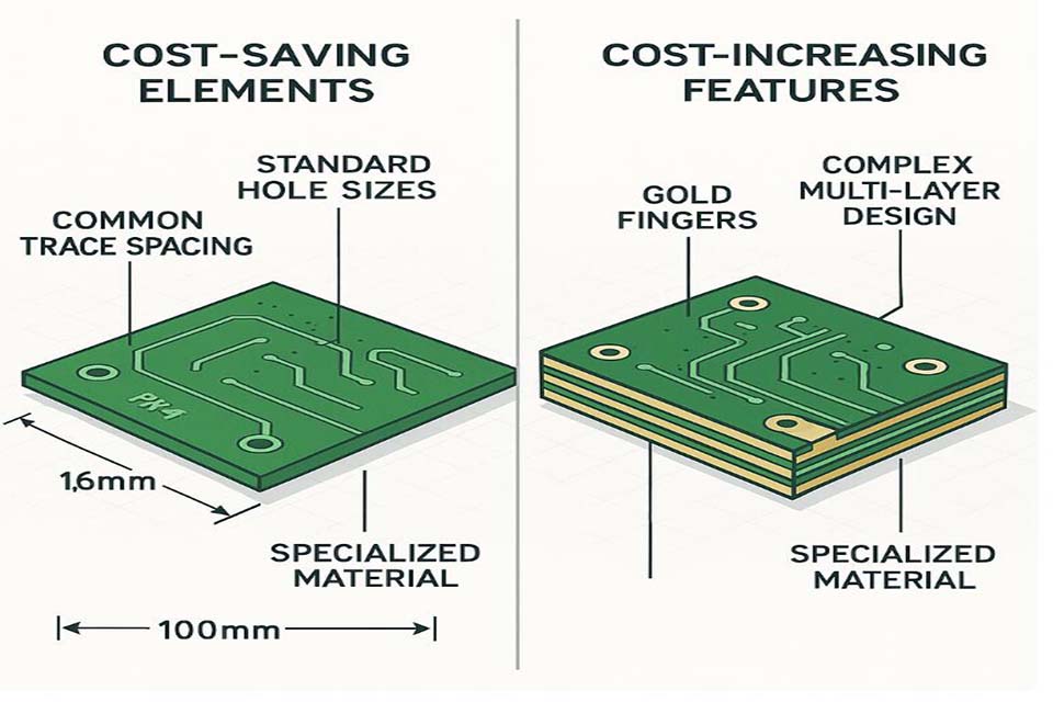
1. Îmbunătățiți dimensiunea și forma tablei
- Suggestion: Keep your board as tiny as feasible and use a standard rectangle-shaped or square form.
- Why it Conserves Money: PCB cost is directly symmetrical to its location. Uneven or intricate shapes (like L-shapes or circles) call for additional milling/routing, which adds cost and lowers the number of boards can fit on a basic production panel.
2. Reduceți numărul de straturi
- Idea: Utilize the fewest layers possible. A 4-layer board can be 50-70% much more pricey than an equivalent 2-layer board.
- Why it Saves Cash: Each layer includes several production steps (lamination, pressing, drilling, plating), significantly increasing complexity and cost. Just move from 2 to 4 layers if definitely necessary for signal stability or density.
3. Respectați criteriul materialului FR-4
- Idea: Unless you have strict high-frequency (RF) or high-temperature demands, make use of the typical FR-4 substrate.
- Why it Conserves Cash: FR-4 is one of the most common, mass-produced, and least expensive PCB product. Specialized materials like Rogers, Teflon, or polyimide are orders of magnitude a lot more costly.
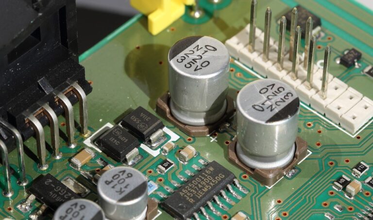
4. Utilizați grosimea plăcii de cerințe
- Suggestion: Layout for the sector basic density of 1.6 mm (0.062″) .
- Why it Conserves Money: Manufacturers supply 1.6 mm cores in enormous amounts. Requesting a non-standard thickness (e.g., 0.8 mm or 2.0 mm) requires special materials and procedure adjustments, adding cost and lead time.
5. Evită traseele și spațiile ultra-fine
- Tip: Maintain your minimum trace size and spacing as large as feasible, ideally 6 mil (0.15 mm) or greater .
- Why it Conserves Cash: Tighter resistances ( = 6 mil effortlessly.
6.Decrease Drill Opening Count and Usage Larger Holes
- Tip: Decrease the number of vias and use bigger drill opening sizes( e.g., > 0.3 mm).
- Why it Saves Money: The boring procedure takes some time. Extra openings indicate even more maker time. Extremely tiny openings( microvias) break drill little bits regularly and call for more expensive, high-RPM makers.
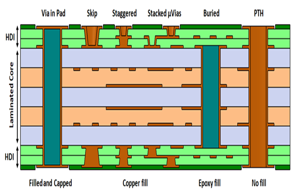
7.Evită Vias Oarbe și Ascunse
- Idea: Use just typical “through-hole” vias that go through all layers of the board.
- Why it Conserves Money: Blind (surface to inner layer) and hidden (internal layer to inner layer) vias call for several, sequential lamination and exploration cycles. This is an extremely pricey and complex procedure scheduled for high-density interconnect (HDI) boards.
8. Selectează cea mai economică suprafață finală
- Idea: For the majority of standard SMT and through-hole applications, HASL (Hot Air Solder Leveling) is the cheapest alternative.
- Why it Conserves Cash: ENIG (Electroless Nickel Immersion Gold) is a lot more costly however essential for really fine-pitch BGA components or press-fit ports. If your layout does not require its monotony or service life, stick with HASL.
9. Greutate standard a cuprului utilizat
- Idea: Design with the basic 1 oz (35 µm) copper weight.
- Why it Conserves Cash: This is one of the most usual and readily offered copper foil thickness. Hefty copper (2 oz or even more) is a special-order product and calls for broader trace/space regulations, boosting price.
10. Respectați stilurile de culoare ale măștii de lipit Criterion
- Suggestion: Utilizare Environment-friendly solder mask.
- Why it Saves Money: Green is the universal default. Makers run massive sets of green boards. Asking for other shades (black, white, red, blue) can sometimes include a small fee or boost preparation because they are run less regularly.
11. Utilizarea serigrafiei pe o singură față
- Idea: If you can fit all necessary component designators and markings on one side, do it.
- Why it Saves Cash: Using a 2nd silkscreen layer is an added manufacturing step. While commonly a little expense, it adds up over big quantities.
Component B: Element & Setting Up (Layout for Setting Up – DFA)
These tips focus on making it less costly and much easier for devices (or individuals) to place and solder parts onto the board.
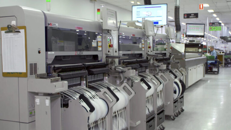
12. Preferă montarea pe suprafață (SMT) în locul montării prin găuri (TH)
- Suggestion: Utilize SMT parts wherever possible.
- Why it Saves Money: SMT setting up is highly automated and fast. Through-hole components typically need manual insertion and a separate wave soldering procedure, which is much more labor-intensive and pricey.
13. Păstrați toate elementele SMT pe o singură parte
- Pointer: When possible, create your board for single-sided assembly.
- Why it Conserves Money: Putting together on both sides needs the board to experience the whole SMT line (solder paste, pick-and-place, reflow oven) two times. This virtually increases the assembly labor and equipment time.
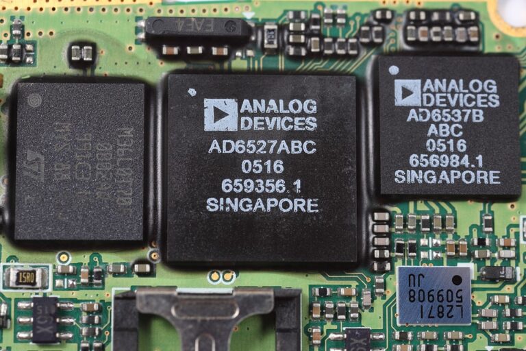
14. Selectați elemente comune, oferite în mod convenabil
- Pointer: Design with generic, multi-source parts (e.g., common resistor/capacitor values, popular microcontrollers, and logic chips).
- Why it Conserves Money: Obscure or single-source parts are a lot more expensive, have long lead times, and posture a huge supply chain risk. Utilize a tool like Octopart or examine distributor supply levels throughout the layout phase.
15. Stay Clear Of Incredibly Tiny Element Bundles
- Suggestion: Make use of 0402 or 0603 plan sizes for easy elements instead of 0201 or smaller sized.
- Why it Saves Cash: While 0201 elements are small, they require a lot more exact (and pricey) assembly tools and have lower returns. 0402 is the sweet spot for expense and thickness for many contemporary assemblers.
16. Offer Ample Component-to-Component Clearance
- Suggestion: Leave space around elements for the pick-and-place nozzle, rework devices, and assessment.
- Why it Saves Money: Densely jam-packed components are tough to area, can create solder bridging, and are almost impossible to remodel or repair, resulting in much more junked settings up.
17. Maintain a Clean and Accurate Costs of Products (BOM)
- Idea: Your BOM ought to be remarkable, with right Supplier Component Figures (MPNs), amounts, and designators.
- Why it Conserves Money: A bad BOM is the # 1 reason for assembly delays and cost overruns. Errors cause incorrect parts being bought and placed, needing pricey rework and job holds.
18. Include Fiducial Markers .
- Suggestion: Location a minimum of 3 fiducial pens on your board, ideally in a triangular pattern.
- Why it Saves Money: These are optical registration marks utilized by the pick-and-place equipment to exactly situate the board. Without them, automated assembly is difficult, compeling costly hand-operated placement.
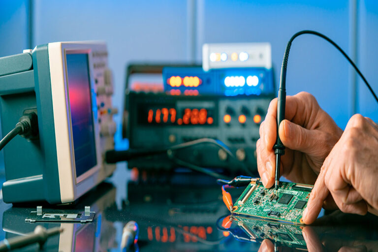
19. Design for Testability (DFT)
- Tip: Include examination factors for important signals (power, clocks, information lines).
- Why it Saves Cash: A board that can not be checked is a black box. Debugging a defective board without test points is extremely time-consuming. A couple of additional pads can save hours of design time and make automated practical testing (FCT) feasible.
20. Layout for Panelization
- Idea: Plan just how your board will certainly be arrayed on a bigger panel. Use V-grooves for rectangle-shaped boards and mouse-bites (tab-routing) for irregular forms.
- Why it Conserves Cash: Assembly residences deal with panels, not single boards. A well-designed panel makes the most of the number of boards per panel and minimizes depanelization labor. Go over panel requirements with your assembler.

Component C: Refine & Logistics
These pointers relate to the overall getting and administration strategy.
21. Leverage Volume Discounts
- Pointer: Order in bigger quantities.
- Why it Saves Money: The per-unit price of a PCB drops dramatically with quantity. The configuration prices (tooling, stencils, maker programs) coincide whether you order 10 boards or 1,000.
22. Prepare For Requirement Turn-around Times
- Suggestion: Prevent thrill orders.
- Why it Saves Money: A 24-hour or 3-day turn costs a considerable costs. Typical turn times (5-10 days) permit the supplier to batch your order with others, which is much more reliable and cheaper for them– and you.
23. Give Comprehensive Paperwork
- Tip: Include clear fabrication and assembly notes in your Gerbers or a separate document. Define layer stackup, regulated insusceptibility, and any type of unique instructions.
- Why it Saves Money: Excellent documents stops ambiguity and expensive mistakes. A maker who needs to quit and email you with questions is a manufacturer that is including delays and run the risk of to your project.
24. Settle Suppliers (Turnkey Assembly)
- Tip: Make use of a solitary distributor for both PCB fabrication and setting up.
- Why it Conserves Money: A complete provider handles the entire procedure, from sourcing parts to final setting up. This removes shipping costs between vendors, decreases your administration expenses, and makes one event in charge of the final top quality.
25. Talk to Your Supplier Early
- Pointer: Send your preliminary design to your selected fab/assembly house for a DFM/DFA review.
- Why it Saves Money: This is one of the most essential idea. They can spot costly style selections before you finalize the layout. A 10-minute discussion can save you hundreds of dollars by pointing out that altering a via size or trace size will move you right into a less costly manufacturing tier.
Întrebări frecvente
What is the most cost-effective PCB size for manufacturing?
PCB designs under 100mm x 100mm typically offer the best pricing advantages due to optimal material utilization and reduced shipping costs. Larger boards incur significant cost penalties through increased material consumption and handling expenses.
How does layer count affect PCB manufacturing costs?
Single and double-layer boards provide the most economical options, with costs increasing substantially for each additional layer. A larger two-layer board often costs less than a smaller four-layer equivalent with identical functionality.
Which PCB material offers the best value for most applications?
FR4 laminated fiberglass provides excellent cost-effectiveness for most applications, offering good mechanical properties and electrical characteristics at competitive prices. Specialty materials like aluminum or ceramic command premium pricing.
How do trace specifications impact PCB manufacturing costs?
Finer trace widths and spacing increase manufacturing complexity and costs through specialized equipment requirements and reduced yields. Standard capabilities typically provide the best cost-performance balance.
What surface finish provides the best cost-performance balance?
Hot Air Solder Leveling (HASL) offers the most economical finish option while providing excellent solderability. Lead-free HASL variants accommodate regulatory requirements with minimal cost increases.
How can order quantity optimization reduce PCB costs?
Production volume dramatically impacts per-unit costs through economies of scale. Price breaks often occur at specific volume thresholds, making strategic quantity planning essential for cost optimization.
Recapitulare
Eficient Stil PCB şi fabricarea de PCB-uri cost optimization requires tactical preparation across numerous measurements. Dimension minimization, layer count optimization, and product option supply the greatest price reduction chances. Requirement specifications generally offer the most effective value recommendation contrasted to customized choices.
Secret cost-saving approaches include:
- Targeting board dimensions under 100mm x 100mm for ideal prices
- Utilizing conventional FR4 products and coatings unless specific demands mandate alternatives
- Minimizing layer count through calculated layout optimization
- Defining trace widths and spacing based upon practical demands instead of aesthetic preferences
- Selecting manufacturers supplying detailed value-added solutions
- Conducting prototype screening prior to full-scale production dedications
- Evaluating total expense of ownership instead of preliminary pricing alone
Inteligent fabricarea de PCB-uri decisions balance instant expense considerations with lasting performance demands. These techniques allow substantial cost financial savings while preserving high quality requirements necessary for reputable digital products.