-
Xinxintian Industrial Zone, Shajing Street,Bao'an District, Shenzhen, China

PCB Design Best Practices: A Guide to Optimizing Your Circuit
[ad_1]
PCB Design Best Practices: A Guide to Optimizing Your Circuit
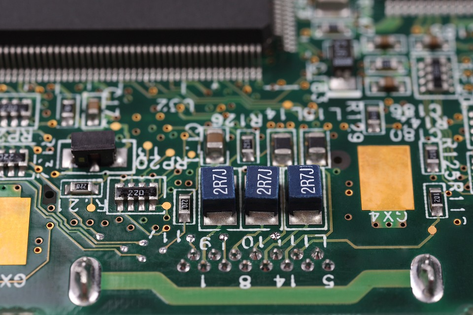
When designing a printed circuit board (PCB), it’s essential to follow best practices to ensure that your circuit is optimized for performance, reliability, and manufacturability. In this article, we’ll explore the key considerations and techniques for designing a high-quality PCB that meets your project’s requirements.
1. Define Your Design Requirements
Before starting your PCB design, it’s crucial to define your design requirements. This includes identifying the type of circuit you’re designing, the components you’ll be using, and the performance specifications you need to meet. This information will help you determine the best design approach and ensure that your PCB meets your project’s needs.
2. Choose the Right PCB Material
The type of PCB material you choose will depend on the application and the components you’re using. For example, if you’re designing a high-frequency circuit, you may need to use a material with low dielectric loss. If you’re designing a circuit that will be exposed to harsh environments, you may need to use a material that’s resistant to moisture and corrosion.
3. Use a Ground Plane
A ground plane is a conductive layer on the PCB that provides a reference point for all the other components. It’s essential to use a ground plane to ensure that your circuit operates correctly and to reduce electromagnetic interference (EMI). The ground plane should be connected to the PCB’s power supply and should be designed to minimize the risk of shorts and electrical noise.
4. Use a Power Plane
A power plane is a conductive layer on the PCB that provides a power supply to the components. It’s essential to use a power plane to ensure that your circuit operates correctly and to reduce the risk of power supply noise. The power plane should be designed to minimize the risk of shorts and electrical noise.
5. Use Decoupling Capacitors
Decoupling capacitors are used to filter out noise and reduce the risk of electrical interference. They should be placed close to the components they’re decoupling and should be connected to the power plane and ground plane. The value of the decoupling capacitor will depend on the frequency of the noise and the components you’re using.
6. Use a Shielded Box
A shielded box is a enclosure that’s designed to reduce electromagnetic interference (EMI). It’s essential to use a shielded box to ensure that your circuit operates correctly and to reduce the risk of EMI. The shielded box should be designed to minimize the risk of electrical noise and should be connected to the ground plane.
7. Use a Thermal Interface Material (TIM)
A thermal interface material (TIM) is a material that’s used to reduce the thermal resistance between the components and the PCB. It’s essential to use a TIM to ensure that your circuit operates correctly and to reduce the risk of overheating. The TIM should be designed to minimize the risk of electrical noise and should be connected to the ground plane.
8. Use a PCB Layout Tool
A PCB layout tool is a software program that’s used to design and layout your PCB. It’s essential to use a PCB layout tool to ensure that your circuit is designed correctly and to minimize the risk of errors. The PCB layout tool should be designed to minimize the risk of electrical noise and should be connected to the ground plane.
9. Use a PCB Fabrication Service
A PCB fabrication service is a company that’s responsible for manufacturing your PCB. It’s essential to use a PCB fabrication service to ensure that your circuit is manufactured correctly and to minimize the risk of errors. The PCB fabrication service should be designed to minimize the risk of electrical noise and should be connected to the ground plane.
10. Test Your PCB
Testing your PCB is essential to ensure that it operates correctly and to identify any errors or defects. It’s essential to test your PCB using a variety of test methods, including functional testing, parametric testing, and visual inspection. The test methods you use will depend on the type of circuit you’re designing and the components you’re using.
Conclusion
In conclusion, designing a high-quality PCB requires careful consideration of a variety of factors, including the type of circuit you’re designing, the components you’re using, and the performance specifications you need to meet. By following the best practices outlined in this article, you can ensure that your PCB is optimized for performance, reliability, and manufacturability.
FAQs
Q: What is the most important factor to consider when designing a PCB?
A: The most important factor to consider when designing a PCB is the type of circuit you’re designing. This will determine the components you’ll be using and the performance specifications you need to meet.
Q: What is the best way to reduce electromagnetic interference (EMI) on a PCB?
A: The best way to reduce EMI on a PCB is to use a shielded box and to minimize the risk of electrical noise. This can be achieved by using a ground plane, a power plane, and decoupling capacitors.
Q: What is the best way to ensure that a PCB is manufactured correctly?
A: The best way to ensure that a PCB is manufactured correctly is to use a PCB fabrication service and to specify the manufacturing requirements clearly. This will ensure that the PCB is manufactured to the correct specifications and that any errors or defects are identified and corrected.
Q: What is the best way to test a PCB?
A: The best way to test a PCB is to use a variety of test methods, including functional testing, parametric testing, and visual inspection. This will ensure that the PCB operates correctly and that any errors or defects are identified and corrected.
Q: What is the most common error that occurs during PCB design?
A: The most common error that occurs during PCB design is a mistake in the component placement or routing. This can be avoided by using a PCB layout tool and by carefully reviewing the design before manufacturing.
Q: What is the best way to minimize the risk of electrical noise on a PCB?
A: The best way to minimize the risk of electrical noise on a PCB is to use a ground plane, a power plane, and decoupling capacitors. This will ensure that the PCB operates correctly and that electrical noise is minimized.
Q: What is the best way to ensure that a PCB is reliable?
A: The best way to ensure that a PCB is reliable is to design it correctly, using a combination of best practices and careful consideration of the components and performance specifications. This will ensure that the PCB operates correctly and that any errors or defects are identified and corrected.
[ad_2]

admin
You may also like

PCB Manufacturing 101: A Beginner’s Guide to Printed Circuit Board Production – A comprehensive overview of the PCB manufacturing process, from design to production.

The Importance of SMT Solder Masking in High-Density PCB Manufacturing
PCB Assembly Design for Manufacturing (DFM): A Guide to Making it Right the First Time