-
Xinxintian Industrial Zone, Shajing Street,Bao'an District, Shenzhen, China
High-Speed PCB Design: Techniques and Considerations for Fast and Reliable PCBs – Strategies for designing PCBs that can handle increased signal speeds and data transfer rates.
[ad_1]
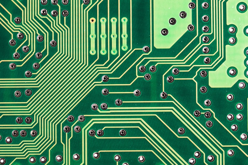
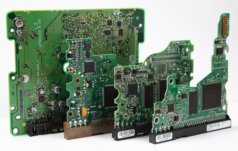
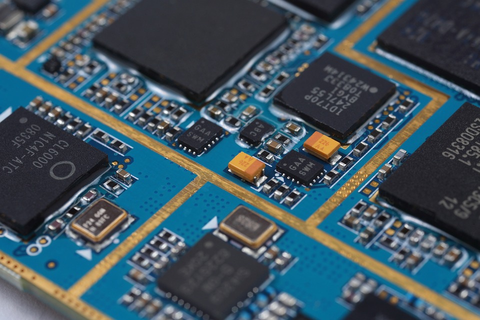
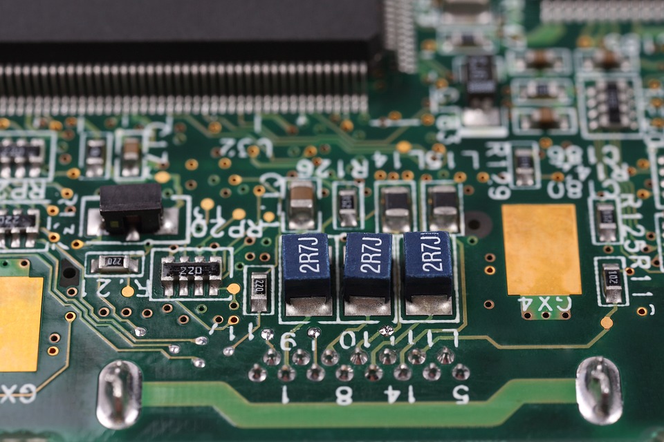
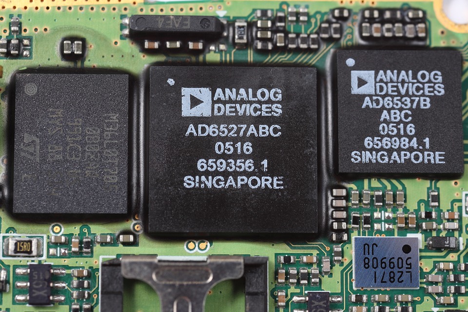
With the increasing demand for faster and more reliable electronic devices, high-speed PCB design has become a crucial aspect of modern electronics. PCBs (Printed Circuit Boards) play a vital role in the functioning of many electronic devices, and their design is critical in determining the overall performance of these devices.
Challenges of High-Speed PCB Design
High-speed PCB design poses several challenges, including:
- Reduced noise and signal integrity issues
- Increased signal integrity
- New and complex routing techniques
- Materials and manufacturing considerations
- Electromagnetic compatibility
To overcome these challenges, high-speed PCB designers must consider a range of techniques and considerations, including:
Design Techniques for High-Speed PCBs
Several design techniques can be employed to design high-speed PCBs that can handle increased signal speeds and data transfer rates:
- Advanced layout techniques, such as silicon-based routing and 3D stacking
- Advanced library components, such as gigabit controllers and advanced logic devices
- Secure manufacturing processes, such as component selection and placement
- Signal integrity analysis and optimization
- Noise reduction techniques, such as shielding and decoupling
These techniques can help ensure that high-speed PCBs are designed and manufactured to meet the demands of modern electronics, without compromising on performance, reliability, and noise reduction.
Considerations for High-Speed PCB Design
Several considerations must be taken into account when designing high-speed PCBs, including:
- Signal integrity analysis and optimization
- Electromagnetic interference (EMI) and radio-frequency interference (RFI) mitigation
- Data transfer rates and data throughput
- Power supply and power distribution network (PDN) design
- Component selection and placement
These considerations are critical in ensuring that high-speed PCBs are designed and manufactured to meet the demands of modern electronics, without compromising on performance, reliability, and noise reduction.
Conclusion
In conclusion, high-speed PCB design is a critical aspect of modern electronics, and requires a thorough understanding of design techniques and considerations. By employing advanced design techniques, such as silicon-based routing and 3D stacking, and considering factors such as signal integrity analysis and optimal component selection, high-speed PCB designers can create reliable and noise-free boards that meet the demands of modern electronics.
FAQs
Q: What are the benefits of high-speed PCB design?
A: High-speed PCB design enables the creation of faster and more reliable electronic devices, with improved signal integrity and reduced noise.
Q: What are some design techniques for high-speed PCBs?
A: Advanced layout techniques, advanced library components, secure manufacturing processes, signal integrity analysis and optimization, and noise reduction techniques can be employed to design high-speed PCBs.
Q: What are some considerations for high-speed PCB design?
A: Signal integrity analysis and optimization, electromagnetic interference (EMI) and radio-frequency interference (RFI) mitigation, data transfer rates and data throughput, power supply and power distribution network (PDN) design, and component selection and placement are all critical considerations for high-speed PCB design.
[ad_2]

admin
You may also like
The Evolution of Printed Circuit Boards: A History of Innovation
The Benefits of Outsourcing PCB Assembly: Is it Right for Your Business?
PCB Assembly for Industrial Control Systems: Ensuring Dependable Performance in Harsh Environments