-
Xinxintian Industrial Zone, Shajing Street,Bao'an District, Shenzhen, China
High-speed PCB and back drilling technology
High-speed PCB design and back drilling technology: the core solution for signal integrity
Abstract In the fields of 5G communication, artificial intelligence servers and high-speed data centers, PCB vias (metallized holes) and backdrilling technology (controllable depth drilling) are key technologies to ensure signal integrity and system reliability. This article systematically analyzes the optimization strategy of via design in high-speed PCBs, the core principles and process flow of backdrilling technology, and combines industry benchmark cases and simulation data to provide engineers with a complete guide from theory to practice, helping high-density and high-frequency circuit design break through performance bottlenecks.
1. High-speed PCB via design: from parasitic effects to optimization strategies
1. Electrical characteristics of vias and signal integrity challenges
As inter-layer connection channels of multi-layer PCBs, vias (Via) have parasitic capacitance and parasitic inductance that significantly affect signal quality in high-frequency scenarios:
• Parasitic capacitance formula:
[ C = 1.41 \cdot \varepsilon_r \cdot T \cdot D_1 / (D_2 – D_1) ] Where (\varepsilon_r) is the dielectric constant, (T) is the board thickness, (D_1) is the pad diameter, and (D_2) is the isolation area diameter.
• Parasitic inductance formula:
[ L = 5.08h \left[ \ln(4h/d) + 1 \right] ] The via length (h) and the aperture (d) directly affect the inductance value. The inductance of a 10mil aperture via can reach 1.2nH at 1GHz, resulting in impedance mutation.
Case: In a PCIe 4.0 design, the via stub length exceeded 200mil, resulting in eye closure. By backdrilling, the stub was controlled to less than 50mil, and the eye opening was increased by 40%.
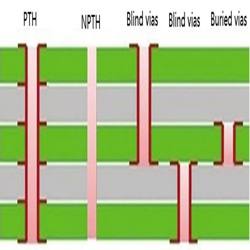
2. Comparison of via types and applicable scenarios
| Type | Structural features | Advantages | Limitations |
|---|---|---|---|
| Through hole | Penetrates the entire board | Low cost, simple process | Long stub, poor high-frequency performance |
| Blind hole | Connects the surface layer and the inner layer | Reduces stubs, suitable for high density | Requires laser drilling, high cost |
| Buried hole | Connection between inner layers | No stub, low signal loss | High manufacturing complexity |
3. Six golden rules for high-speed via design
1.Size optimization:
• General design: 0.25mm/0.51mm/0.91mm (drilling/pad/isolation area);
• High-density board: 0.20mm/0.46mm/0.86mm, with non-through-hole (microvia) technology.
2.Isolation area expansion: follow the D1=D2+0.41 rule to reduce the capacitance effect.
3.Layer routing strategy: reduce the number of layer changes, and use differential symmetrical via layout when necessary.
4.Thin board priority: PCBs with a thickness of ≤1.6mm can reduce parasitic parameters by more than 30%.
5.Power/ground optimization: drill holes nearby, lead length <0.5mm, line width ≥2 times the signal line.
6.Ground via array: place GND vias every 0.5mm in the layer change area to shorten the return path.
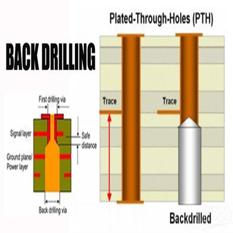
2. Back drilling process: the ultimate solution to eliminate the stub effect
1. Back drilling technology principle and core parameters
Back drilling (Back Drilling) removes unused copper pillars (Stubs) of through holes through secondary drilling.
Key technical indicators include:
• Stub residual length (B value): 50-150μm, for every 10μm increase in residual, the signal loss increases by 0.5dB@10GHz.
• Aperture tolerance: ±0.05mm, high-precision CNC drilling machine is required.
• Depth control: using micro-current sensing technology, positioning accuracy reaches ±5μm.
Process flow:
- Primary drilling → 2. Electroplating sealing → 3. Outer layer pattern production → 4. Back drilling positioning → 5. Secondary drilling → 6. Water washing and chip removal.
2. Four major advantages of backdrilling technology
• Improved signal integrity:
•reduce reflection and resonance:and reduce the bit error rate (BER) to below 10⁻¹².
• Cost-effectiveness: replace 50% of blind and buried hole requirements and reduce lamination complexity.
• EMI suppression: reduce radiated noise by 6-8dB, and pass FCC Class B certification.
• Design flexibility: support ultra-high-speed scenarios such as 112G PAM4 optical modules.
3. Industry application cases
• Communication base station: Huawei 5G AAU board uses back drilling technology to control the stub within 80μm and the insertion loss is <0.3dB/mm@28GHz.
• Data center: NVIDIA A100 GPU carrier board is optimized through backdrilling, and the PCIe 5.0 signal rate is increased to 32GT/s.
• Aerospace: Lockheed Martin satellite PCB uses back drilling + low-loss materials to ensure signal stability under extreme temperatures.
III. Simulation verification and future technology trends
1. Simulation-driven via optimization
• Tool recommendation:
• Ansys HFSS: Full-wave electromagnetic field analysis of via S parameters and field distribution;
• Cadence Sigrity: Time domain reflection (TDR) verification of impedance continuity.
• Case: A DDR5 design found the clock via delay deviation through simulation, and the jitter was reduced from 15ps to 8ps after optimization.
2. Technology frontiers and challenges
• Ultra-high frequency materials: The dielectric constant (Dk) of Rogers RO4500 series boards is as low as 3.0, which can reduce via capacitance by 30%.
• Laser back drilling: The accuracy is improved to ±10μm, supporting 0.1mm aperture processing.
• 3D packaging integration: TSV through silicon via technology combined with PCB back drilling to achieve heterogeneous integrated packaging.
Summary
In the high-speed digital era, via design and back drilling process are the core levers for PCB performance breakthroughs. By accurately controlling parasitic parameters, optimizing stub length, and combining advanced simulation tools (such as Keysight ADS), engineers can solve the signal integrity problems of cutting-edge technologies such as 112G PAM4 and DDR6. In the future, with material innovation and process upgrades (such as Sevenpcba‘s nano-level back drilling solution), PCBs will continue to evolve towards higher frequencies and higher integration.