-
Xinxintian Industrial Zone, Shajing Street,Bao'an District, Shenzhen, China
Designing for Success: A Beginner’s Guide to PCB Design Best Practices
[ad_1]
Designing for Success: A Beginner’s Guide to PCB Design Best Practices
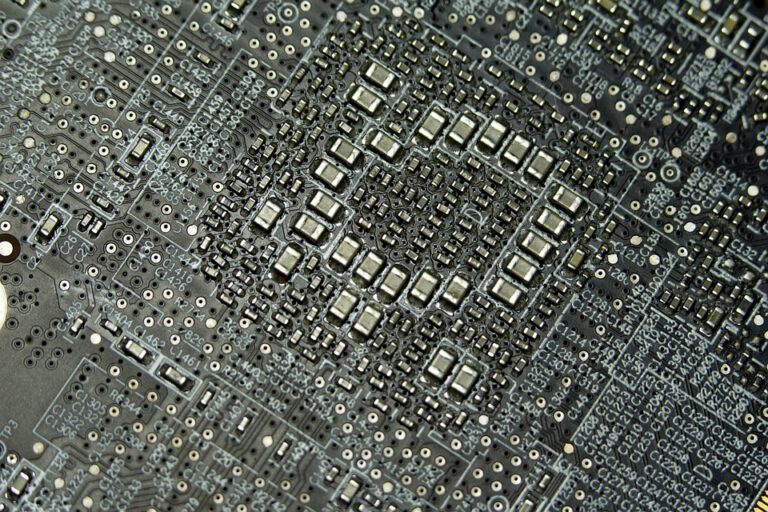
PCB design is a crucial step in the development of electronic products. A well-designed PCB can ensure the reliability, performance, and manufacturability of the final product. However, designing a PCB can be a daunting task, especially for beginners. In this article, we will provide a beginner’s guide to PCB design best practices, covering the essential steps and considerations to ensure success.
Step 1: Define the Project Requirements
The first step in designing a PCB is to define the project requirements. This includes identifying the type of product, its functionality, and the desired performance. It is essential to gather all the necessary information from the stakeholders, including the product specifications, electrical requirements, and mechanical constraints.
Some of the key considerations when defining the project requirements include:
- Product functionality and features
- Electrical requirements, such as voltage, current, and frequency
- Mechanical constraints, such as size, shape, and mounting
- Environmental considerations, such as temperature, humidity, and vibration
Step 2: Choose the Right Software
There are many PCB design software options available, each with its own strengths and weaknesses. When choosing the right software, consider the following factors:
- Ease of use: Look for software with an intuitive interface and user-friendly features.
- Feature set: Consider the software’s ability to handle complex designs, including routing, component placement, and simulation.
- Cost: Evaluate the software’s cost, including any licensing fees or subscription costs.
- Community support: Look for software with an active community and good customer support.
Some popular PCB design software options include:
- Altium Designer
- OrCAD
- KiCad
- Autodesk Eagle
Step 3: Create a Design Plan
Once you have chosen the right software, it’s time to create a design plan. This includes defining the design requirements, creating a bill of materials (BOM), and establishing a design schedule.
Some of the key considerations when creating a design plan include:
- Design requirements: Define the design requirements, including the product’s functionality, electrical requirements, and mechanical constraints.
- BOM: Create a BOM that includes all the necessary components, including their quantities, descriptions, and part numbers.
- Design schedule: Establish a design schedule that includes milestones, deadlines, and resource allocation.
Step 4: Design the PCB
With the design plan in place, it’s time to start designing the PCB. This includes creating the PCB layout, placing components, and routing signals.
Some of the key considerations when designing the PCB include:
- Component placement: Place components in a way that minimizes signal integrity issues and ensures proper thermal management.
- Signal routing: Route signals in a way that minimizes noise and ensures proper signal integrity.
- Power distribution: Ensure proper power distribution by placing power planes and vias strategically.
Step 5: Simulate and Verify the Design
Once the PCB design is complete, it’s essential to simulate and verify the design to ensure it meets the project requirements. This includes simulating the PCB’s electrical performance, thermal performance, and mechanical performance.
Some of the key considerations when simulating and verifying the design include:
- Electrical simulation: Simulate the PCB’s electrical performance to ensure it meets the project requirements.
- Thermal simulation: Simulate the PCB’s thermal performance to ensure it meets the project requirements.
- Mechanical simulation: Simulate the PCB’s mechanical performance to ensure it meets the project requirements.
Conclusion
Designing a PCB requires careful planning, attention to detail, and a thorough understanding of the design requirements. By following the best practices outlined in this article, you can ensure a successful PCB design that meets the project requirements and is manufacturable.
FAQs
Q: What is the most important step in designing a PCB?
A: The most important step in designing a PCB is defining the project requirements. This includes identifying the type of product, its functionality, and the desired performance.
Q: What is the best PCB design software for beginners?
A: The best PCB design software for beginners is KiCad. KiCad is free, open-source software that is easy to use and has a large community of users and developers.
Q: How do I ensure proper signal integrity in my PCB design?
A: To ensure proper signal integrity in your PCB design, place components in a way that minimizes signal integrity issues, route signals in a way that minimizes noise, and use signal integrity analysis tools to identify and fix issues.
Q: What is the most common mistake made in PCB design?
A: The most common mistake made in PCB design is not simulating and verifying the design before manufacturing. This can lead to costly rework and delays in production.
Q: How do I ensure proper thermal management in my PCB design?
A: To ensure proper thermal management in your PCB design, place heat sinks and thermal vias strategically, use thermal simulation tools to identify hotspots, and ensure proper airflow around the PCB.
[ad_2]

admin
You may also like
PCB Design for Manufacturability (DFM): A Comprehensive Guide
PCB Assembly for Dummies: A Beginner’s Guide to Understanding the Process

PCB Design Software: A Comparison of Popular Tools and Features