-
Xinxintian Industrial Zone, Shajing Street,Bao'an District, Shenzhen, China
Design for Testability (DFT) in PCBs: Maximizing Testability and Minimizing Debugging Time
[ad_1]
Design for Testability (DFT) in PCBs: Maximizing Testability and Minimizing Debugging Time
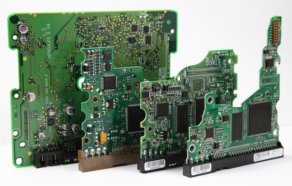
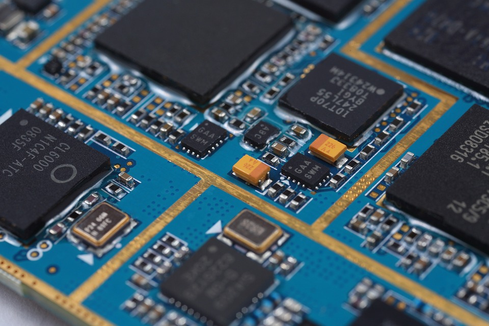
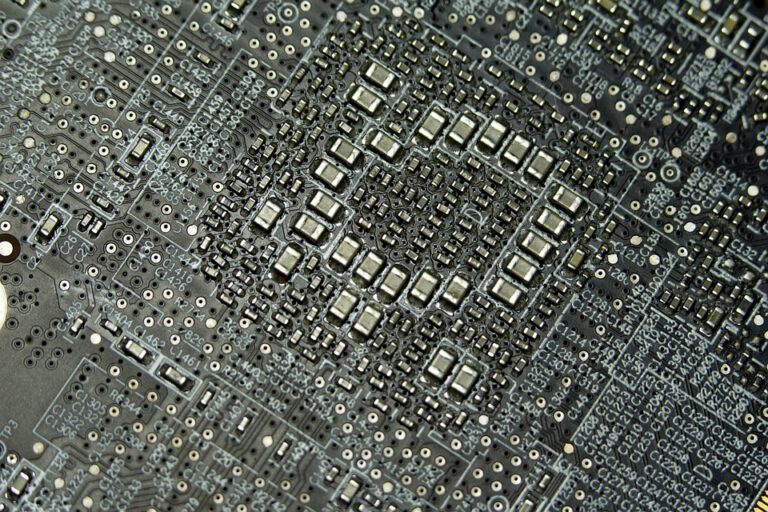
As the complexity of printed circuit boards (PCBs) continues to increase, the need for effective testability solutions has become more pressing than ever. One of the primary challenges in PCB design is ensuring that the board is designed in a way that makes it easy to test and debug. Design for Testability (DFT) is an essential approach to achieving this goal.
In this article, we will discuss the key aspects of DFT in PCBs, highlighting the benefits, challenges, and best practices for implementing DFT in your PCB design process. We will also explore the impact of DFT on debugging time and how it can help minimize the time spent on debugging.
What is Design for Testability (DFT)?
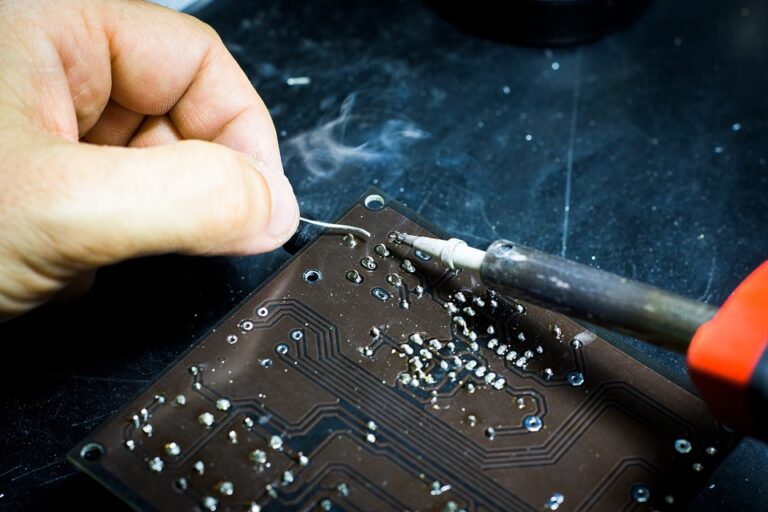
Design for Testability (DFT) is a design approach that focuses on making it easier to test and debug PCBs. It involves a set of principles, techniques, and best practices that aim to simplify the testing process, reduce testing time, and improve test coverage. In essence, DFT is about designing the board in a way that allows for easy diagnosis and isolation of faults, making it easier to identify and fix errors.
Benefits of DFT
The benefits of DFT are numerous, but some of the most significant advantages include:
- Reduced debugging time: By designing the board with testability in mind, debugging time can be significantly reduced, resulting in cost savings and faster time-to-market.
- Improved test accuracy: DFT ensures that all parts of the board can be effectively tested, reducing the likelihood of missed defects and improving overall test coverage.
- Increased reliability: By identifying and fixing defects early on, DFT can help reduce the risk of defects propagating to the end product, leading to increased reliability.
Challenges and best practices in DFT
While the benefits of DFT are well-known, there are some challenges and best practices to keep in mind when designing PCBs with DFT in mind:
Challenges:
- Balancing testability with functionality: It can be difficult to strike a balance between designing the board for testability and ensuring it still meets the desired functionality.
- Compliance with industry standards: Compliance with industry standards, such as IEEE 1450-1999, can be challenging, especially for companies new to DFT.
Best practices:
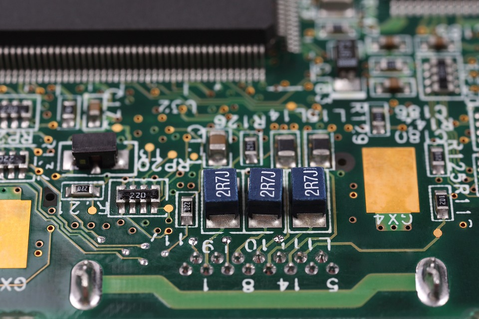
- Use modular design: Breaking down the board into smaller modules can help reduce complexity and make it easier to test and debug.
- Use boundary-scan testing: Adding a boundary-scan controller to the board can simplify testing and debugging.
- Implement test points: Including test points in the design can make it easier to test and debug specific components or sections of the board.
- Use automated testing tools: Utilizing automated testing tools, such as automated fault insertion (AFI), can speed up the testing process and improve accuracy.
Impact of DFT on debugging time
The impact of DFT on debugging time is significant. By designing the board with testability in mind, debugging time can be reduced by up to 50%. This is because DFT makes it easier to identify and isolate faults, reducing the time spent debugging and improving overall productivity.
Conclusion
In conclusion, Design for Testability (DFT) is a critical aspect of PCB design that can have a significant impact on debugging time and overall product reliability. By understanding the benefits, challenges, and best practices of DFT, designers and engineers can create PCBs that are easier to test and debug, reducing the time and cost associated with debugging. Whether you’re working on a complex system-on-module (SoM) or a simple prototype board, incorporating DFT principles will help ensure that your board is designed with testability in mind from the outset.
FAQs
- What is the primary benefit of Design for Testability (DFT)?
The primary benefit of DFT is to make it easier to test and debug PCBs, reducing debugging time and improving overall test coverage. - What are some common challenges associated with DFT?
Some common challenges include balancing testability with functionality, and ensuring compliance with industry standards. - What are some best practices for DFT?
Some best practices include using modular design, implementing boundary-scan testing, adding test points, and using automated testing tools. - How does DFT impact debugging time?
DFT can reduce debugging time by up to 50%, making it easier to identify and isolate faults.
[ad_2]

admin
You may also like

A Guide to PCB Component Selection: Choosing the Right Components for Your Design
PCB Design for Manufacturability (DFM): A Comprehensive Guide
Why Outsource Your PCB Assembly? The Benefits of Professional Manufacturing Services