Una guida per il processo ibrido da SMT
Tecnologia di assemblaggio
Riassunto: La tecnologia di assemblaggio SMT dei PCB sta subendo cambiamenti rivoluzionari, con lo sviluppo di prodotti elettronici orientati all'essenzialità, alla compattezza e all'alta densità. L'articolo approfondisce i principali processi della tecnologia a montaggio superficiale (SMT), della tecnologia Through-Holl (THT) e dei processi di assemblaggio ibridi, integrando le norme ISO 9001, ISO 13485 e 6110G per illustrare le 9 fasi principali e le 4 strategie di controllo qualità della produzione di PCBA. Introducendo le pratiche di gestione intelligente della catena di approvvigionamento del ConsumerPCBA, fornisce alle aziende produttrici di componenti elettronici una soluzione a ciclo completo, dall'adattamento del progetto alla produzione su larga scala, che contribuisce a migliorare l'efficienza produttiva e la resa del prodotto di oltre 301 TP5T.
Sommario
I. Sviluppo della tecnologia di assemblaggio PCB SMT e processo chiave
1. Tecnologia di montaggio superficiale (SMT): punto di riferimento per una costruzione accurata
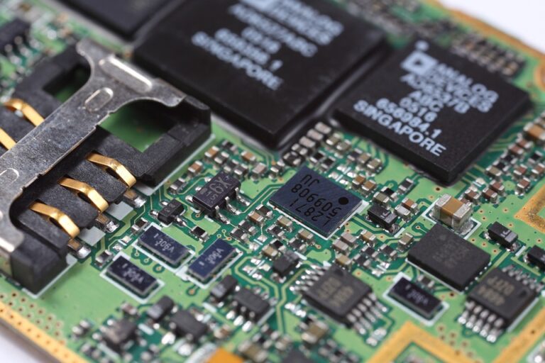
• Processo SMT Realizza perfettamente posizionamenti collettivi elevati di microcomponenti (dimensioni 01005) tramite apparecchiature automatizzate. I suoi principali vantaggi includono:
• Posizionamento a livello di micron: la precisione del posizionamento utilizzando un sistema di allineamento visivo raggiunge ± 25μm
• Saldatura senza piombo: pasta saldante SN96.5/Ag3.0/Cu0.5 conforme a ROHS, punto di maltaggio 217 ℃
• capacità produttiva di competenze Capacità artigianale di plassemth mispainch
Diagramma di flusso del processo:
2. Holl Technology (THT): una scelta che privilegia l'affidabilità
1. La tecnica THT è adatta per dispositivi e connettori ad alta potenza e le sue caratteristiche includono:
• Vantaggio di dissipazione del calore: adatto per dispositivi di dissipazione del calore come il pacchetto TO-220 e la resistenza termica è ridotta di 15%
• Compatibilità del processo: la tecnologia di saldatura ad onda selettiva realizza saldature locali e riduce il consumo energetico di 30%
3. Assemblaggio SMT PCB ibrido: la soluzione definitiva per la progettazione di PCB complessi
Nel campo delle stazioni base 5G e dell'elettronica per l'automotive, l'assemblaggio ibrido realizza un salto di prestazioni attraverso una strategia di ottimizzazione a tre ordini:
Pianificazione del layout: progettazione delle partizioni SMD e THT, spaziatura ≥ 2,5 mm per prevenire interferenze termiche Sequenza di saldatura: prima la saldatura a riflusso e poi la saldatura a onda per evitare danni secondari dovuti ad alte temperature Coordinamento del rilevamento: la stazione di rilavorazione a raggi X + BGA risolve il problema dei giunti di saldatura nascosti
II.Analisi completa del processo di assemblaggio PCBA SMT e controllo di qualità
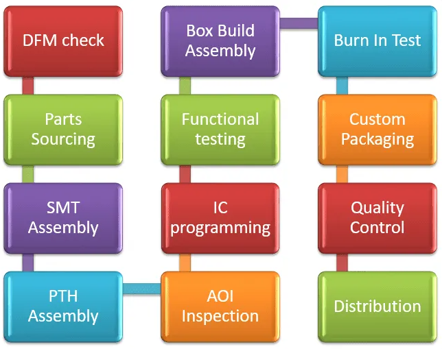
1. 9 fasi fondamentali del processo (basate sullo standard IPC-J-STD-001)
| Passi | Parametri tecnici chiave | Punti di controllo qualità |
|---|---|---|
| Cottura su tavola nuda | 125℃/4h, umidità <5%RH | Elimina lo stress del substrato e previene l'esplosione della scheda |
| Stampa con pasta saldante | Spessore della maglia d'acciaio 0,1-0,15 mm | Copertura di rilevamento SPI ≥98% |
| Posizionamento dei componenti | Precisione del componente 0402 ±0,03 mm | Pressione dell'ugello regolabile 0,5-1,2 N |
| Saldatura a riflusso | Temperatura massima 245±5℃, tempo 60-90s | Monitoraggio in tempo reale di 100 punti di misurazione della temperatura |
| Rilevamento AOI | Tasso di riconoscimento dei difetti ≥99,7% | Tasso di falsi allarmi dell'algoritmo di apprendimento profondo <0,3% |
| Saldatura ad onda | Altezza dell'onda di saldatura 8-12 mm | Protezione dell'azoto contenuto di ossigeno <100 ppm |
| Processo di pulizia | Detergente acquoso pH 6,5-7,5 | Contaminazione ionica <1,56μg/cm² |
| Test funzionale | Velocità del test della sonda volante 200 punti/secondo | Copertura del test 100% |
| Rivestimento conforme | Spessore del rivestimento 20-50μm | Prova di nebbia salina ≥500 ore senza corrosione |
Innovazione fondamentale del processo: nel campo dell'elettronica per autoveicoli, la tecnologia di riflusso sotto vuoto può eliminare le bolle BGA e ridurre il tasso di vuoti da 5% a meno di 0,5%.
III. Standardizzazione dei documenti ed esercizio di produzione intelligente
1. Requisiti del documento di progettazione (standard IPC-2581)
• File Gerber: 32 livelli di segnale + 16 definizioni di livello di potenza includono
• ODB++: integra la distinta base e i dati del modello 3D, il tasso di superamento dell'ispezione DFM è aumentato del 40%
• Specifiche del disegno di assemblaggio: errore di identità polare del componente <0,5 mm, copertura del progetto a prova di esplosione 100%
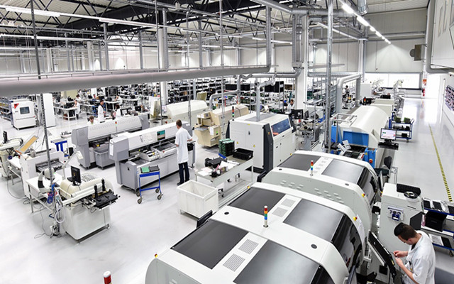
2. Sistema di produzione intelligente del PCBA di consumo
Creare un vantaggio competitivo attraverso quattro nuove tecnologie:
- Digital Twin: il debug virtuale ha ridotto il ciclo di introduzione del nuovo prodotto da 30%
- Material Smart Cloud Warehouse: inventario in tempo reale di oltre 100.000 SKU, tempo di risposta agli avvisi di carenza <2 ore
- Previsione della qualità dell'IA: in base a un database di difetti di livello milione, la precisione della previsione della resa raggiunge 95%
- Produzione ecologica: processo senza piombo + sistema di riciclaggio delle acque reflue, emissioni di carbonio ridotte del 45%
Caso del cliente: un produttore di apparecchiature mediche ha ottenuto un incremento di 60% nella densità mediante l'adattamento di un assemblaggio misto e i suoi prodotti hanno ottenuto la certificazione medica IEC 60601–1.
IIII. 7 criteri per selezionare 7 fornitori di PCBA SMT di alta qualità
- Sistema di certificazione: ISO 9001+ IPC -A -610 Classe 3 Doppia certificazione
- Capacità di processo: packaging CSP con passo 0,3 mm e supporto per scheda HDI a 20 strati
- Garanzia di consegna: prototipo veloce in 48 ore, ordine in lotti puntuale 99%
- Controllo dei componenti: agente autorizzato originale + autenticità mediante rilevamento a raggi X
- Capacità di test: con un set completo di ICT, FCT, apparecchiature di screening dello stress ambientale
- Assistenza tecnica: il team di analisi DFM ha un'esperienza media di oltre 8 anni
- Adattamento dei costi: il sistema di analisi dei costi BOM aiuta i clienti a ridurre i costi di 15%-30%
Riepilogo e approccio
La tecnologia di assemblaggio dei PCB si sta evolvendo verso l'intelligenza artificiale (Industria 4.0), l'alta densità (componenti integrati) e il rispetto dell'ambiente (mix di origine biologica). Covenant aiuta i clienti a raggiungere i seguenti obiettivi costruendo una piattaforma digitale full-link di "design-testing":
• Tasso di primo passaggio (FPY) aumentato da 85% a 98%
• Ciclo di crescita dei nuovi prodotti ridotto di 40%
• Costi di produzione su larga scala ridotti di 25%