Suggerimenti completi per la progettazione di assemblaggio PCB dal produttore cinese di PCBA
Astratto
This article presents a detailed methodology for pcb assembly design (PCBA), emphasizing the integration of manufacturing constraints into the electronic design process.
The guide navigates from fundamental concepts like schematic integrity and Bill of Materials (BOM) management to advanced layout considerations such as high-speed signal routing, power plane design, and thermal dissipation techniques. A significant portion is dedicated to the practical application of Design for Manufacturability (DFM) and Design for Assembly (DFA) principles, including panelization, fiducial placement, solder mask considerations, and component clearances.
It also covers the generation of a complete manufacturing data package, including Gerbers, BOM, and Centroid files. The objective is to equip design engineers with the knowledge to create robust PCBAs that meet performance specifications while being optimized for high-yield, low-cost automated assembly.
Sommario
PCB Assembly design Guide
PCBs, or printed circuit boards, are the unsung heroes of modern electronics. Most users have no idea how the components in the electronic devices they know and love work together. But for engineers, OEMs, and designers, there is a lot to know and a lot to learn about PCBs. This PCB design guide was written to help both new and experienced engineers make smarter design decisions early on, resulting in the perfect components for their products. Let’s start with the basics:
1. Cos'è un PCB?
IL circuito stampato or PCB is the heart of any electronic device. It has two main functions: Housing electronic components, connecting components for operation The board itself is made of a non-conductive substrate, such as fiberglass, that is coated with copper on one or both sides. The copper conducts electricity and is etched away from the board, leaving the appropriate components to connect to each other through the circuit.
2. Scheda PCB PCBA. PCA. Qual è il nome corretto per una scheda a circuito stampato con tutti i componenti?
There are many acronyms used by industry experts for printed circuit boards. The most vexing question is, what is the difference between PCB and PCBA? Here is a breakdown of what they mean: PWB – Printed Wiring Board. The first term used when the connection of electronic components was simply point-to-point circuit work. PCB – Printed Circuit Board. Technically, the term PCB refers to the etched wiring board itself without any components mounted on it. Since printed circuit design often affects device functionality, the IPC Technical Executive Committee designated this term in 1999 as a term for new document development.
PCA – Printed Circuit Assembly. For clarity, it is used after the 1999 IPC change. PCBA – Printed Circuit Board Assembly. It is a printed circuit board with all the electronic components mounted on it. PCB is the most popular term when referring to the whole, assembled. When communicating with manufacturers and external suppliers, it is important to clarify what type of PCB is required – basic board or fully connected printed board assembly (PCBA). For an in-depth look at all the acronyms used for printed circuit boards, check out discussions by industry experts and more.
3. Come funzionano i circuiti stampati?
PCBAs are designed to provide a central hub for integrating all the electronic components in a device together. The board is created using multiple layers, with conductive paths or lines laminated to the substrate material. These copper traces are used to conduct electricity, acting as a circuit for all the components soldered to the board, thus powering the device, while providing insulation and safe current transfer.
4. Di cosa sono fatti i PCB?
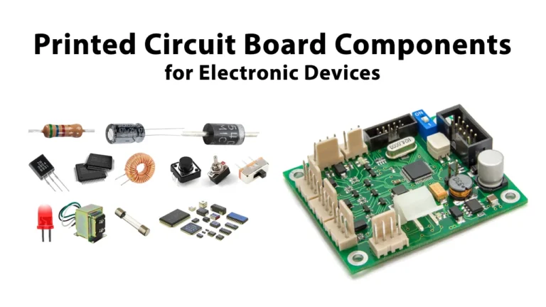
Each PCB hardware component plays a vital role in powering an electronic device. PCB components include:
- What are PCBs made of? The board itself consists of four key components: Substrate – The foundation of the PCB, the substrate is usually made of fiberglass or some other non-conductive material. The substrate can be single-layer or multi-layer. Copper – Used to carry electrical current, copper in PCBs replaces electrical wires.
Solder Mask – Metal used to create connections between the surface of a PCB and electronic components. The solder mask protects the electronic traces underneath from adverse conditions.
Silkscreen – Layer used to mark the connecting lines of electronic components, warnings, and other features unique to a device.
Before moving to final PCB production, prototypes must be verified to ensure that all components are connected and working properly to power the device.
6. What are the different types of PCBs?
To accommodate the design, application, and complexity of a device, several design decisions need to be made upfront. What type of PCB is needed first? Just like light guides, PCBs can be either rigid or flexible, depending on the design and application of the device.
Rigid PCBs – Designed to not bend or deviate from their original shape or position.
Flexible PCBs – Can be folded, twisted, and bent into the desired configuration. They are thinner, lighter, and can accommodate unique shapes.
Flexible PCB vs. Rigid Cost
From a cost perspective, here’s how the two compare:
Rigid PCBs
Typically a more cost-effective solution because they are easy to mass produce due to automation.
Flexible PCB Printed Circuit Boards Eliminate the need for additional connectors, which can reduce overall production costs. However, they require additional steps to secure components and automated assembly, which makes them cost-prohibitive. When choosing between rigid or flexible PCBs, cost is not the only determining factor – design constraints such as weight and space can also come into play. Layers of PCBs Single-layer PCBs Boards made from a single layer of substrate or base. Typically, one side of the substrate is coated with a thin layer of metal on one side of the base. Single-layer PCBs are ideal for rapid production due to their simple design and ease of automation.
Double-layer PCBs Boards that contain soldered electrical connections on both sides. This is achieved when copper or other conductive materials are applied to both sides of the board. For added flexibility, double-sided PCBs can utilize through-hole or surface mount (SMT) designs. Multi-layer PCBs When used for more complex designs, multi-layer boards include four or more layers. Other benefits of multi-layer PCBs are a smaller footprint and fewer wiring harnesses, which reduces overall weight. These PCBs are ideal for aerospace, handheld devices, battery and signal transmission, and many other applications.
7. Quali sono i vantaggi dell'utilizzo di un circuito stampato?
PCBs offer a number of benefits to engineers, OEMs, and designers of electronic devices, including: Minimal space requirements – Because all electronic connections are on the board, there is no need for multiple wires to carry current and take up valuable space on the device. Simplified installation and troubleshooting – All components are mounted on the PCB and clearly labeled for easy access during assembly and maintenance.
Simplified assembly – PCBs allow for quick assembly compared to other means (e.g., wired connections). Secure placement and connectivity – With PCBs, all electronic components are soldered to the board to ensure they stay in place. Manufacturing efficiency – When mass production is required, PCBs are more cost-effective than other connection methods. Reliable operation – The design of PCBs ensures stable operation because connections are made through copper wires that will not come loose.
8. Di che colore è il circuito stampato?
It may seem like it’s the substrate that determines the color of the PCB, but it’s actually the solder mask. The substrate is usually green, but the solder mask over it can be blue, yellow, orange, purple, red, black, white, and of course, green.
9. Il colore del PCB è importante?
There are many reasons to choose one, such as a specific color for the PCB substrate – whether it is branding, or if the system is pre-produced in one color and the boards produced are another color. In addition, some colors are easier to see contrast than with the naked eye, which can be an advantage when inspecting the board. However, if lighting is to be used, choosing a white surface for the PCB can help reflect light. In some cases, this additional control can provide more LED choices to optimize the design.
Depending on the application, sometimes it may be necessary to reflect light. In these applications, white PCBs are ideal. White PCBs are often used in LED light engines or LED lighting systems. On the other hand, there may be applications where light reflection is not desired, such as DJ equipment used in a dark nightclub. The color of the substrate is just one of the factors to consider during the schematic stage of PCB design.
- What is the PCB design process like? There are eight processes involved in the manufacture of printed circuit boards, which can vary in complexity depending on the design of the device: PCB Design Basics (Simple List)
- Concept of the Electronic Device
- Electronic Schematic Creation
- PCB Layout Design
- Final Bill of Materials (BOM)
- Prototype the PCB
- Evaluate the Prototype
- Install Firmware/Programming
- Full Production The production process consists of the following steps:
- Progettazione PCB
- Print the Copper of the Inner Layers
- Remove Excess Copper
- Inspection and Layer Alignment
- Lamination of the Layers
- Drilling
- PCB Plating
- RoHS Compliance
11. Quanto tempo ci vuole per progettare e produrre un PCB personalizzato?
The turnaround time for custom PCBs depends on the vendor selected, as well as the complexity and volume of the project.
Our PCB capabilities start with design and end with final completion, and we are able to deliver turnaround services in as little as four weeks.
Dedicated warehouse space and advanced tools such as 3D printers enable our team to provide rapid prototyping and speed up the process.
6 Domande frequenti poste regolarmente (Domande frequenti)
Qual è la distinzione tra un PCB e un PCBA?
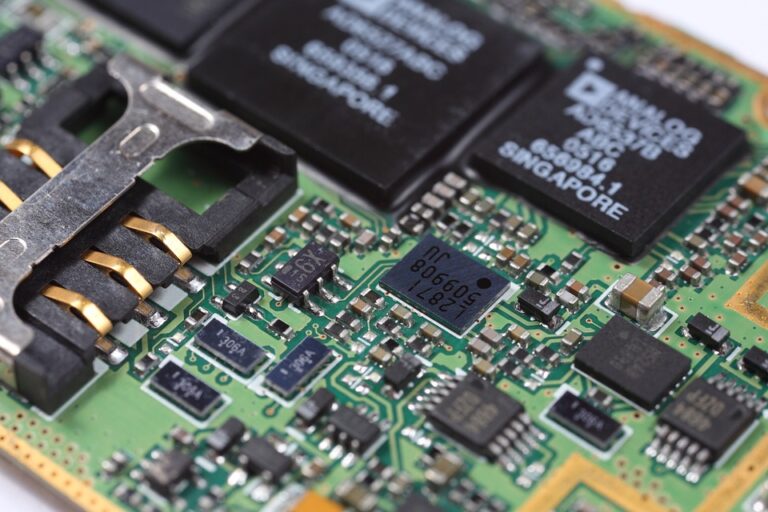
A Printed Circuit Board (PCB) is the bare, unpopulated board, including only the copper traces and substrate. A Printed Circuit Board Assembly (PCBA) is the complete board after all the electronic components (like resistors, ICs, and capacitors) have actually been soldered onto it. This overview focuses on making for the setting up process.
Perché lo Style for Manufacturability (DFM) è così vitale nell'assemblaggio di PCB?
Style for Manufacturability (DFM) is the practice of creating an item for simplicity of manufacturing. In PCBA, applying DFM concepts assists to stop setting up issues, rise production return, reduced expenses, and shorten the moment to market by resolving possible fabrication issues during the design stage.
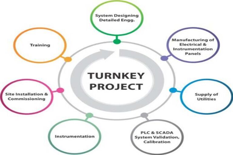
Quali sono i dati necessari per un ordine PCBA?
To have your board constructed, producers normally need three crucial sets of data:.
Gerber Info: Define the copper layers, solder mask, and silkscreen of the PCB.
Expense of Materials (BOM): Details every element, its part number, and its recommendation designator.
Centroid Data (Pick-and-Place File): Gives the X-Y works with and rotation for every component, which is used to configure the automated assembly makers.
Quali sono i fattori vitali da considerare per il posizionamento dei componenti nel layout PCBA?
Appropriate component positioning is vital for performance and assembly. Key factors to consider consist of organizing relevant components, ensuring correct orientation for soldering (e.g., wave or reflow), offering adequate clearance in between parts, managing thermal paths, and keeping signal paths as brief as possible.
Cosa sono i costi dei prodotti (BOM) e perché devono essere esatti?
A Bill of Products (BOM) is a thorough listing of all the raw products, elements, and assemblies required to develop a PCBA. An exact BOM is vital due to the fact that any kind of errors– such as inaccurate component numbers, amounts, or descriptions– can bring about the wrong parts being acquired and positioned, creating production delays and pricey rework.
come posso prevenire problemi comuni di configurazione come tombstoning o ponti di saldatura?
Several typical setting up problems can be protected against during the design stage. Issues like tombstoning (where an element lifts on one end) and solder bridges are often triggered by imbalanced thermal pads or wrong solder mask definitions. Our guide information the details style guidelines for impacts and solder masks to make certain a robust and trustworthy soldering procedure.
Riepilogo:
Il percorso da uno schema elettronico a uno totalmente utile Circuito stampato L'impostazione (PCBA) è piena di possibili sfide che possono portare a costose modifiche e ritardi nella produzione. Questa panoramica funge da roadmap vitale, collegando l'importante vuoto tra il layout digitale e la produzione fisica per garantire che il tuo lavoro sia un successo fin dal primo modello.
Concentrandosi su passaggi pratici e attuabili, questo breve articolo sfata l'intero processo di stile PCBA. Ci spostiamo oltre la teoria dei circuiti fondamentali per coprire gli elementi cruciali che assicurano che la tua scheda possa essere costruita in modo efficiente e affidabile.
Argomenti chiave trattati in questa guida:
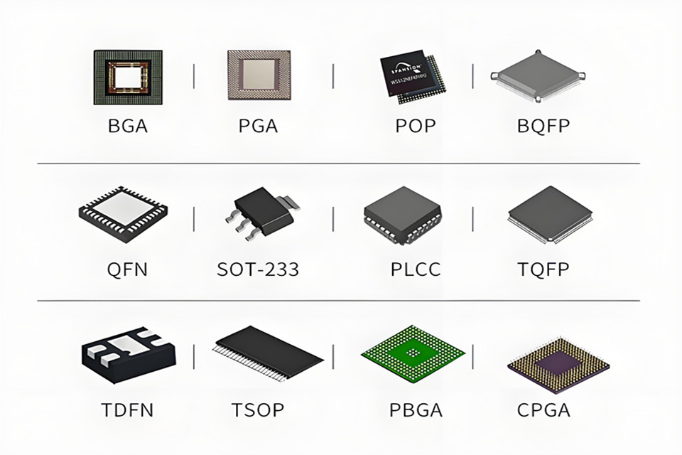
- Fondamenti di PCBA Stile: impara ad avviare correttamente il tuo progetto sviluppando uno schema pulito e una distinta base specifica (Distinta base). Trattiamo le migliori tecniche per la scelta dei componenti, considerando fattori come disponibilità, costo e tipo di confezione per l'impostazione automatizzata.
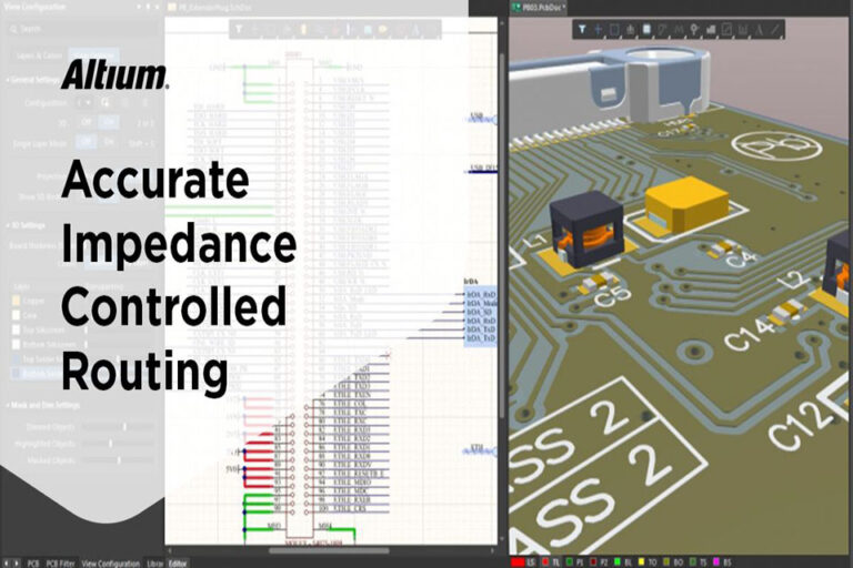
- Strategico Progettazione PCB E Posizionamento dei componenti: Scopri come posizionare i componenti per prestazioni e producibilità ottimali. Questa sezione descrive in dettaglio le tecniche per la gestione della dissipazione termica, garantendo l'integrità del segnale per i circuiti ad alta velocità e organizzando il layout per migliorare la procedura di impostazione.
- Padroneggiare lo stile per la producibilità (DFM e DFA): Questo è il fulcro dell'efficacia PCBA layout. Forniamo un elenco dettagliato per lo stile per la producibilità (DFM) e il layout per l'impostazione (DFA), che copre le normative vitali per le distanze degli elementi, il layout dell'impronta, i requisiti della maschera di saldatura, le tecniche di pannellizzazione e l'uso corretto dei contrassegni di riferimento.
- Il pacchetto di informazioni sulla produzione finale: Evita errori di comunicazione con il tuo fornitore. Questa panoramica spiega in modo specifico come generare un pacchetto di informazioni completo e preciso, incluso Gerber documenti per la fabbricazione, un aggiornato Distinta base per l'acquisto e un Centroide (Pick-and-Place) file per l'assemblaggio automatizzato.
Comprendendo i concetti di questa guida, sarai attrezzato per progettare PCBA robusti, economici e ad alte prestazioni. Imparerai ad anticipare gli ostacoli alla produzione, a proteggerti dai comuni problemi di impostazione e a ottimizzare il percorso dal layout a un prodotto completo.