-
Xinxintian Industrial Zone, Shajing Street,Bao'an District, Shenzhen, China
10 Tips for Designing an Efficient and Reliable Printed Circuit Board – Expert advice on designing a PCB that meets functional and reliability requirements.
[ad_1]
10 Tips for Designing an Efficient and Reliable Printed Circuit Board
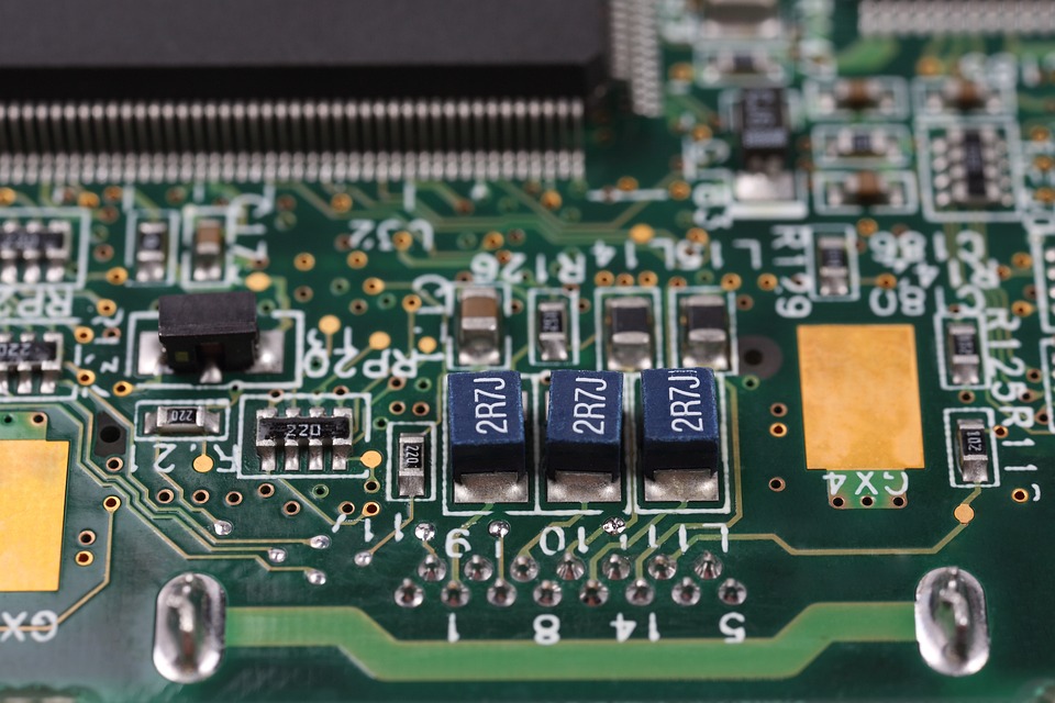
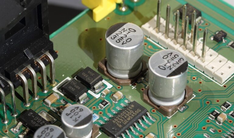
Designing a printed circuit board (PCB) that meets both functional and reliability requirements can be a challenging task. With the increasing complexity of modern electronic devices, it’s essential to ensure that your PCB design is efficient, reliable, and meets the required specifications. In this article, we’ll provide expert advice on designing a PCB that meets your needs.
Tip 1: Define Your Requirements
Before starting your PCB design, it’s crucial to define your requirements. Identify the functional and performance requirements of your PCB, including the type of components, power supply, and signal integrity. This will help you create a clear design specification and ensure that your PCB meets the required standards.
Tip 2: Choose the Right Materials
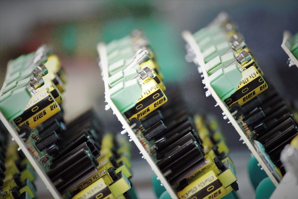
The choice of materials for your PCB is critical to its performance and reliability. Select materials that meet your design requirements, such as FR4, FR5, or high-frequency materials. Consider factors like thermal conductivity, dielectric constant, and moisture absorption when selecting your materials.
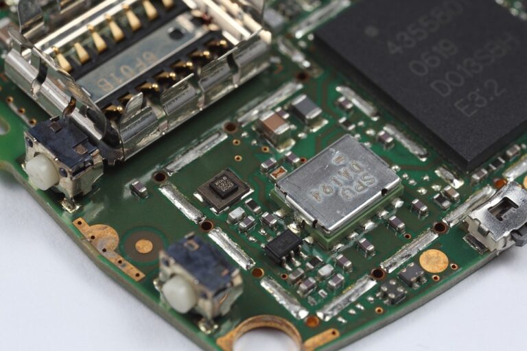
Tip 3: Optimize Component Placement
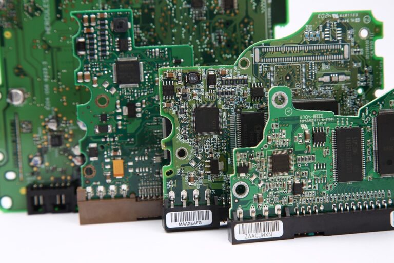
Component placement is a critical aspect of PCB design. Optimize your component placement to minimize signal integrity issues, reduce thermal stress, and improve manufacturability. Use design rules and constraints to ensure that your components are placed correctly.
Tip 4: Use a Ground Plane
A ground plane is a critical component of a reliable PCB design. It helps to reduce electromagnetic interference (EMI), improve signal integrity, and provide a stable reference point for your components. Use a solid ground plane or a grid of vias to ensure a reliable connection.
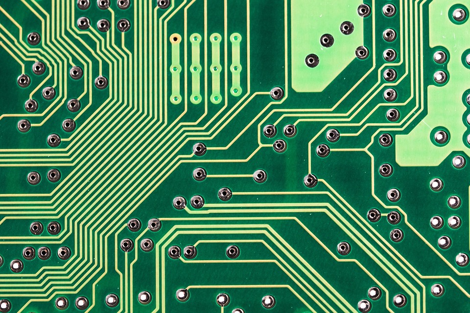
Tip 5: Minimize Via Count
Vias can be a source of signal integrity issues and thermal stress. Minimize your via count by using surface-mount components, optimizing component placement, and using blind and buried vias when necessary.
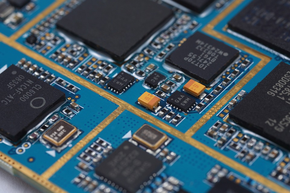
Tip 6: Use Decoupling Capacitors
Decoupling capacitors are essential for reducing noise and improving signal integrity. Use decoupling capacitors to filter out high-frequency noise and ensure that your signals are clean and reliable.
Tip 7: Ensure Proper Thermal Management
Thermal management is critical for ensuring the reliability of your PCB. Ensure that your design allows for proper heat dissipation, using thermal pads, heat sinks, and thermal interfaces to manage heat generation.
Tip 8: Use a Robust Power Distribution Network
A robust power distribution network is essential for ensuring the reliability of your PCB. Use a distributed power supply, decoupling capacitors, and a robust power plane to ensure that your components receive a stable and reliable power supply.
Tip 9: Test and Verify Your Design
Testing and verifying your design is critical for ensuring that your PCB meets your requirements. Use simulation tools, such as SPICE or finite element analysis, to simulate your design and identify potential issues. Verify your design using prototyping and testing.
Tip 10: Collaborate with Experts
Collaborating with experts is essential for ensuring that your PCB design meets your requirements. Work with experienced PCB designers, engineers, and manufacturers to ensure that your design is optimized for performance, reliability, and manufacturability.
Conclusion
Designing a reliable and efficient printed circuit board requires careful consideration of various factors, including component placement, material selection, and thermal management. By following these 10 tips, you can ensure that your PCB design meets your functional and reliability requirements. Remember to define your requirements, choose the right materials, optimize component placement, and test and verify your design to ensure that your PCB is reliable and efficient.
FAQs
Q: What is the most critical aspect of PCB design?
A: The most critical aspect of PCB design is ensuring that your design meets your functional and reliability requirements. This includes defining your requirements, choosing the right materials, and optimizing component placement.
Q: What is the best way to reduce signal integrity issues?
A: The best way to reduce signal integrity issues is to optimize component placement, use a ground plane, and minimize via count. Additionally, use decoupling capacitors and a robust power distribution network to ensure that your signals are clean and reliable.
Q: How can I ensure that my PCB design is reliable?
A: To ensure that your PCB design is reliable, use simulation tools to simulate your design, verify your design using prototyping and testing, and collaborate with experts to ensure that your design is optimized for performance, reliability, and manufacturability.
Q: What is the most common mistake made in PCB design?
A: The most common mistake made in PCB design is neglecting to define the requirements and choosing the wrong materials. This can lead to a design that does not meet the required specifications and is unreliable.
Q: How can I improve the thermal management of my PCB design?
A: To improve the thermal management of your PCB design, use thermal pads, heat sinks, and thermal interfaces to manage heat generation. Additionally, ensure that your design allows for proper heat dissipation and use simulation tools to simulate thermal performance.
[ad_2]

admin
You may also like
SMT vs. Through-Hole: Which Component Mounting Technique is Best for Your PCB?
Printed Circuit Board Failure Analysis: How to Troubleshoot and Repair
How PCB Assembly Services Can Help You Scale Your Business: Benefits and Cost Savings