-
Xinxintian Industrial Zone, Shajing Street,Bao'an District, Shenzhen, China

The Evolution of Printed Circuit Boards: A Brief History – A look back at the development of PCBs from their early beginnings to modern day technology.
[ad_1]
The Evolution of Printed Circuit Boards: A Brief History
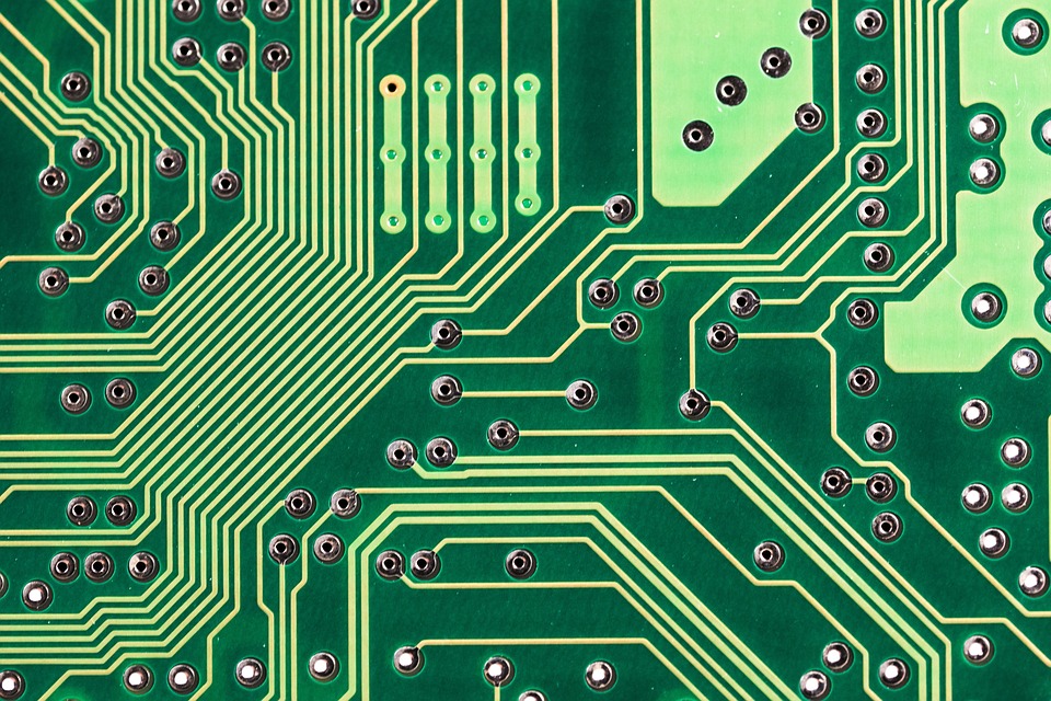
In the early 20th century, electronic devices were bulky and unreliable, with components connected by wires and cables. The development of printed circuit boards (PCBs) revolutionized the industry, allowing for smaller, more efficient, and more reliable electronic devices. In this article, we’ll take a look back at the evolution of PCBs from their early beginnings to modern day technology.
Early Beginnings
The first PCBs were developed in the 1930s by a team of engineers at the Western Union company. They created a circuit board made of a thin layer of copper foil glued to a piece of paper. This early design was limited in its capabilities, but it laid the foundation for future developments.
In the 1940s and 1950s, PCBs began to gain popularity as the demand for electronic devices increased. Companies like IBM and RCA developed their own PCB designs, using materials like bakelite and mica to create the circuit boards.
The Advent of Photolithography
In the 1950s, the development of photolithography revolutionized the PCB industry. This process involved using light-sensitive chemicals to create patterns on the circuit board, allowing for more complex designs and higher density components.
One of the pioneers of photolithography was a company called IBM, which developed a process called “wet etching.” This process involved using a chemical solution to etch the copper foil, creating the desired pattern on the circuit board.
The Rise of Multilayer PCBs
In the 1960s and 1970s, the development of multilayer PCBs became more widespread. This design involved stacking multiple layers of circuit boards on top of each other, allowing for more complex designs and higher density components.
One of the key innovations of this era was the development of the “inner layer” technology. This allowed for the creation of complex circuit boards with multiple layers, increasing the density of components and improving the overall performance of the device.
The Advent of Surface Mount Technology
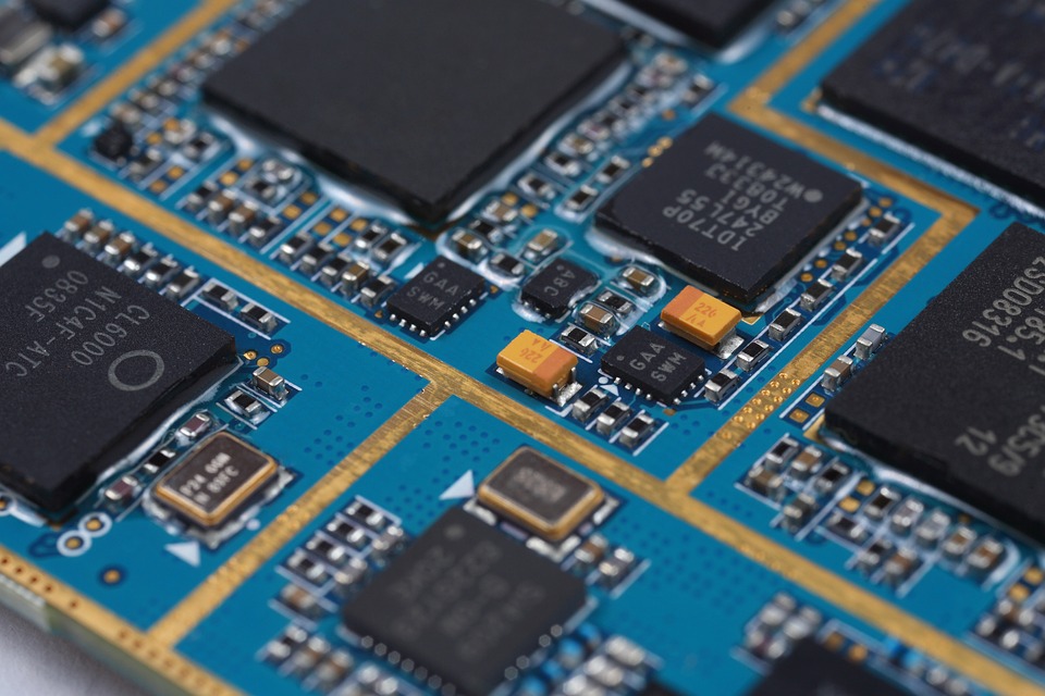
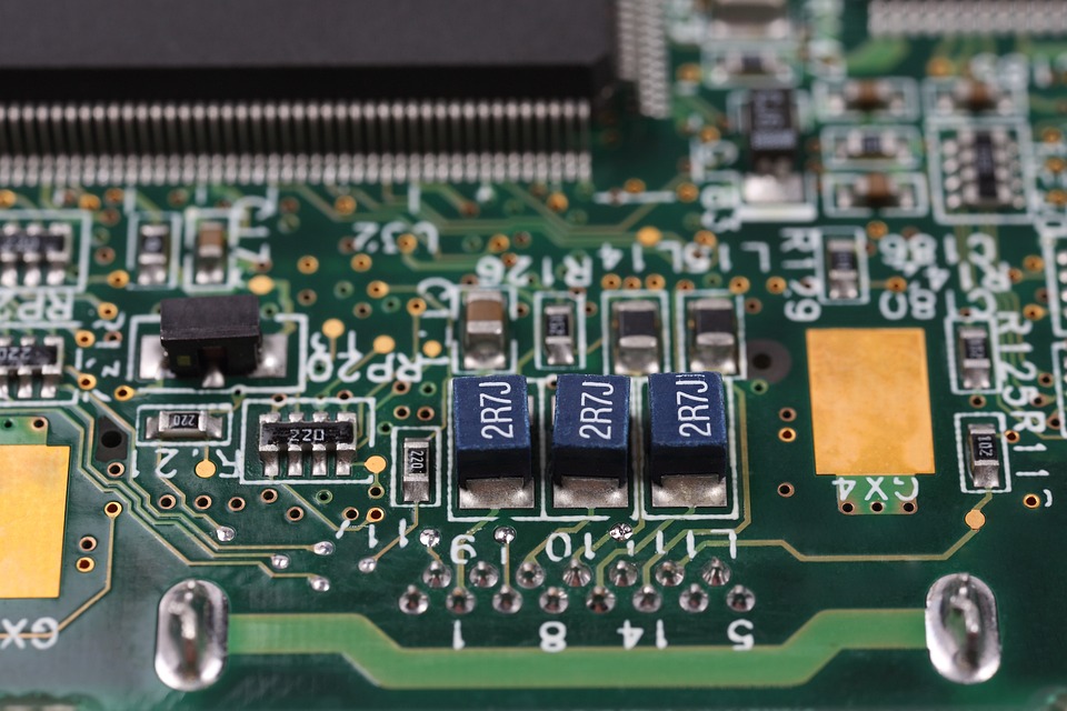
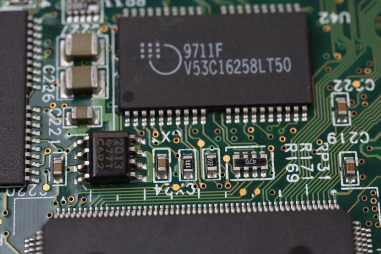
In the 1980s, the development of surface mount technology (SMT) revolutionized the PCB industry. This process involved mounting components directly onto the surface of the circuit board, rather than through-hole mounting.
SMT allowed for the creation of smaller, more compact devices, and improved the overall reliability of the PCB. It also enabled the use of smaller components, such as surface mount devices (SMDs), which further increased the density of components on the circuit board.
Modern Day PCBs
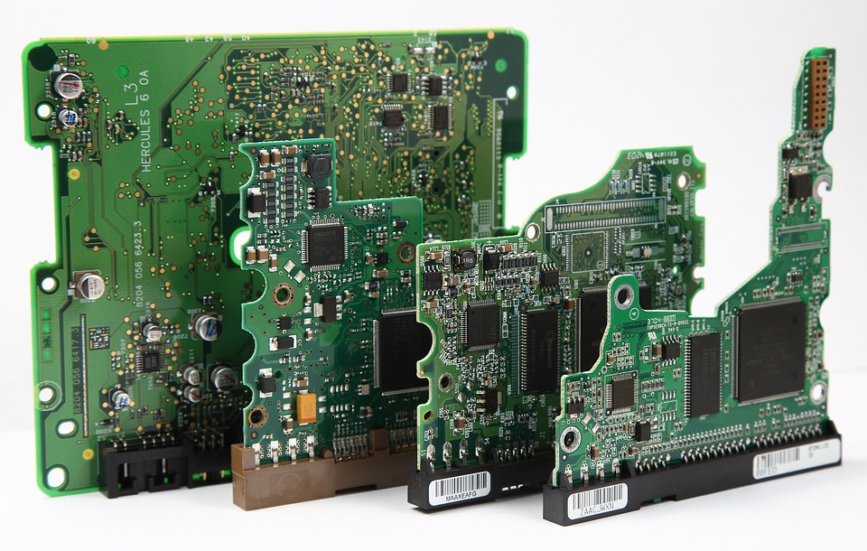
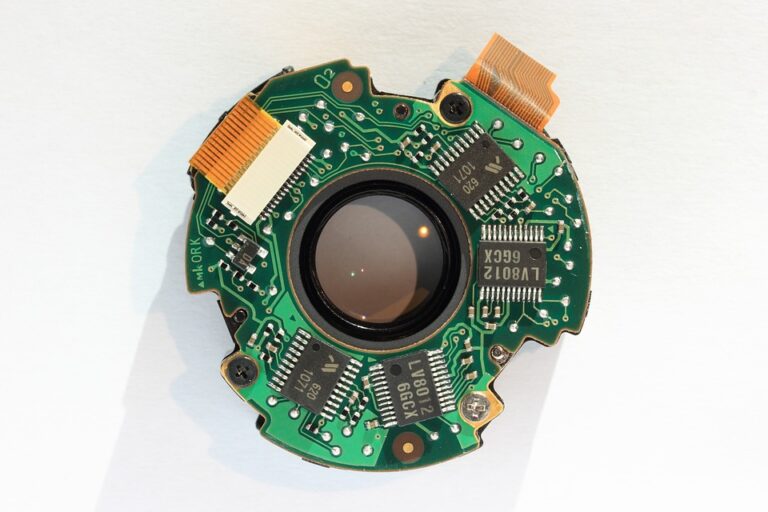
Today, PCBs are used in a wide range of applications, from consumer electronics to medical devices to aerospace technology. Modern PCBs are designed using advanced software and manufacturing techniques, allowing for the creation of complex designs with high density components.
Some of the key trends in modern PCB design include:
- Increased use of SMT and SMDs
- Development of new materials and technologies, such as flexible PCBs and flexible displays
- Increased focus on reliability and durability
- Use of advanced manufacturing techniques, such as 3D printing and laser drilling
Conclusion
The evolution of printed circuit boards has been a long and complex process, driven by advances in technology and changes in the needs of the industry. From their early beginnings in the 1930s to the modern day, PCBs have played a crucial role in the development of electronic devices and have enabled the creation of smaller, more efficient, and more reliable devices.
As the industry continues to evolve, it’s likely that we’ll see even more innovative developments in PCB design and manufacturing. Whether it’s the use of new materials, advanced manufacturing techniques, or new technologies, the future of PCBs is bright and exciting.
FAQs
Q: What is the difference between a PCB and a printed circuit assembly (PCA)?
A: A PCB is a single layer of circuit board material, while a PCA is a complete electronic device that includes multiple components mounted onto a PCB.
Q: What is the purpose of a PCB?
A: The purpose of a PCB is to provide a means of connecting electronic components together, allowing for the creation of complex electronic devices.
Q: What is the most common type of PCB material?
A: The most common type of PCB material is FR4 (flame retardant 4), a type of fiberglass-reinforced epoxy.
Q: What is the difference between SMT and through-hole mounting?
A: SMT involves mounting components directly onto the surface of the PCB, while through-hole mounting involves inserting components through holes in the PCB.
Q: What is the future of PCBs?
A: The future of PCBs is likely to involve the use of new materials, advanced manufacturing techniques, and new technologies, such as flexible PCBs and flexible displays.
Q: How are PCBs manufactured?
A: PCBs are manufactured using a variety of techniques, including photolithography, etching, and drilling. The specific manufacturing process can vary depending on the type of PCB being produced.
Q: What is the cost of a PCB?
A: The cost of a PCB can vary widely, depending on the size, complexity, and materials used. Simple PCBs can cost as little as a few dollars, while complex PCBs can cost tens of thousands of dollars.
Q: Can PCBs be recycled?
A: Yes, PCBs can be recycled. Many companies offer PCB recycling services, which involve disassembling the PCB and separating the components and materials for reuse or recycling.
[ad_2]

admin
You may also like
Material Choices: How to Select the Right PCB Materials for Your Next Project – A guide to understanding the different materials used in PCB construction and tips for selecting the right one for your project.

The Importance of SMT Solder Masking in High-Density PCB Manufacturing
PCB Assembly for Industrial Control Systems: Ensuring Dependable Performance in Harsh Environments