-
Xinxintian Industrial Zone, Shajing Street,Bao'an District, Shenzhen, China
PCB Design for Manufacturing (DFM): Streamlining the Design-to-Manufacturing Process
[ad_1]
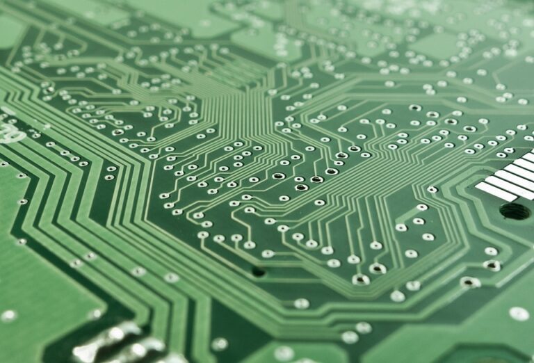
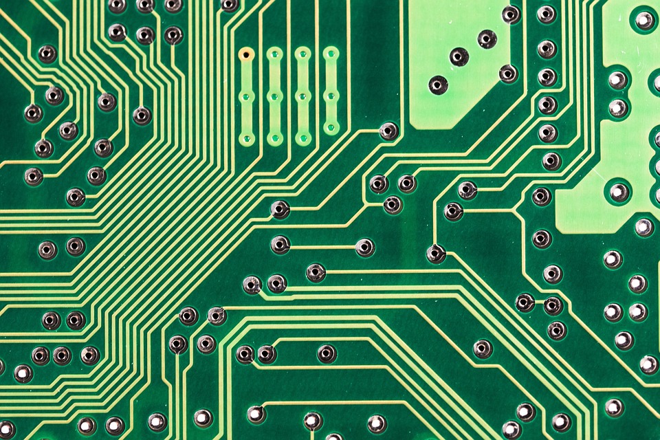
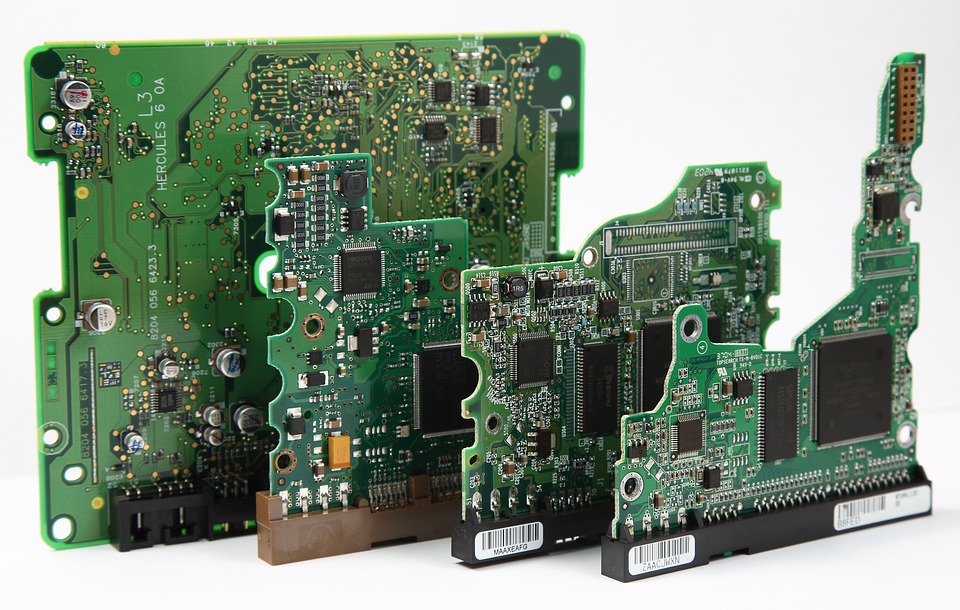
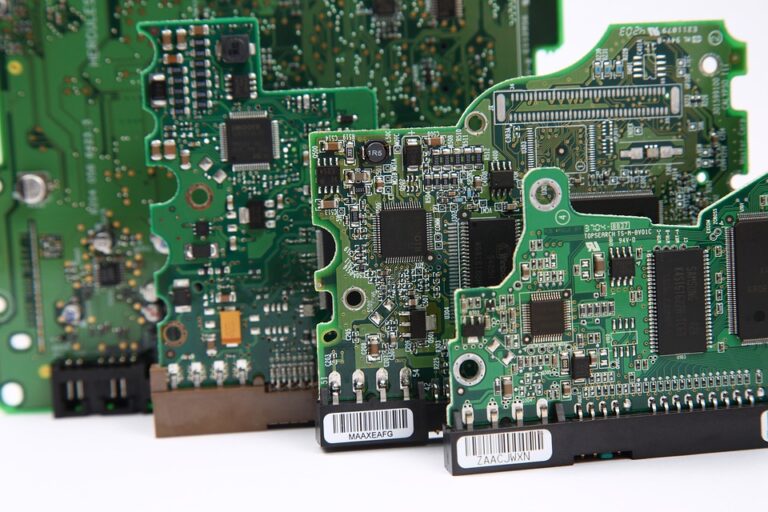
The electronic components of modern technology have become an integral part of our daily lives. From smartphones to laptops, tablets, and desktops, there is an ever-growing demand for high-quality printed circuit boards (PCBs) that are efficient, reliable, and cost-effective. The design-to-manufacturing (DfM) process plays a crucial role in ensuring the smooth production of such PCBs.
In this era of digital transformation, PCBs have become more complex, with a multitude of components, signal integrity, and thermal management requirements. Designers face numerous challenges in creating PCBs that meet the demands of sophisticated electronic systems. Design for manufacturing (DFM) techniques have emerged as a solution to these challenges, streamlining the design-to-manufacturing process for optimum quality, reliability, and reduced costs.
DFM is an extended design process that considers the manufacturing capabilities and constraints of the PCB fabricator. This approach ensures that the design is optimized for ease of manufacturing, reducing subsequent modifications and rework. Effective DFM implementation involves identifying design constraints, optimizing layout, and minimizing design complexity.
PCB design for manufacturing typically commences with the development of a detailed design specification, highlighting required features, performance metrics, and any design-for-manufacturability (DFM) considerations. The design process begins with the creation of a base design, which is then modified to accommodate DFM constraints.
Conducting thermal analysis is an essential part of the DFM process. Thermal analysis helps designers identify potential thermal management issues, allowing for proactive design modifications to mitigate these issues. This ensures optimal heat dissipation, reducing the risk of thermal-related failures and increasing the overall reliability of the PCB.
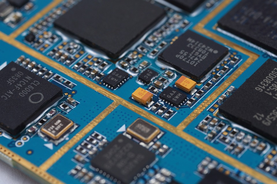
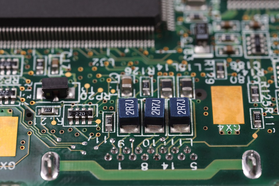
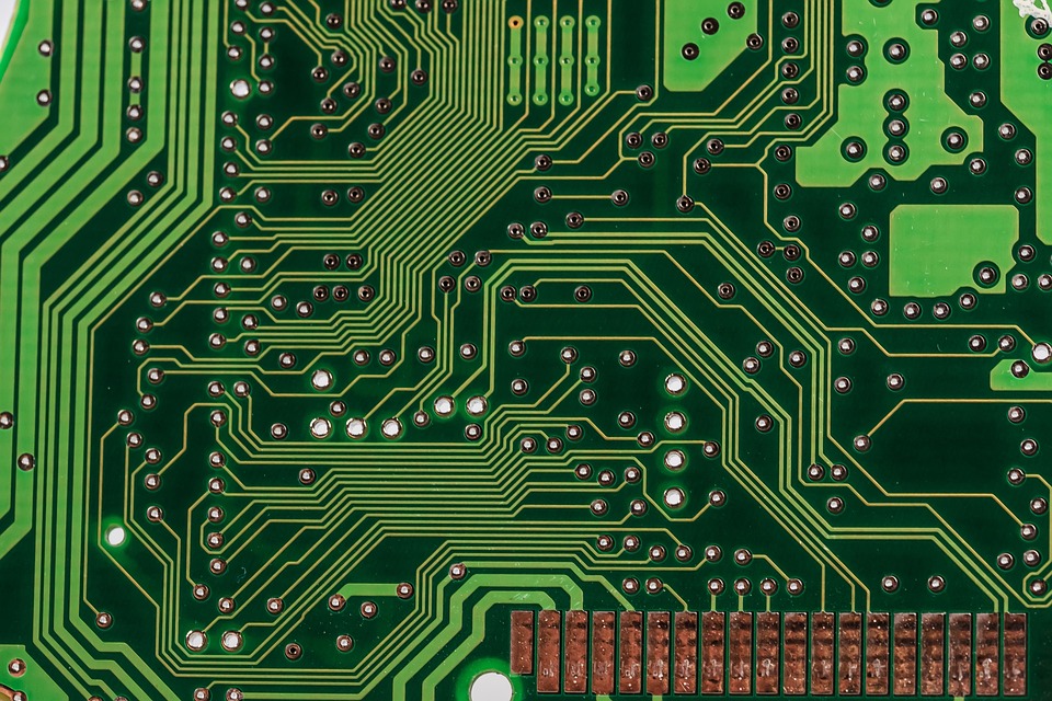
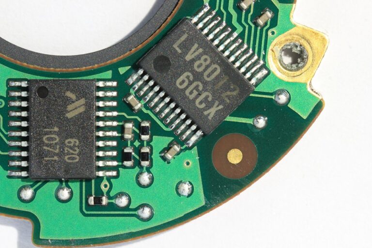
Design for manufacturability techniques can be applied to various PCB architectures, including single-layer and multi-layer boards. These techniques include:
* Right-angle components: Orientation of components to facilitate easy inspection and placement
* Balanced signal integrity: Integrated lines, ground planes, and signal traces to minimize signal reflections
* Electromagnetic interference (EMI) considerations: Careful planning and mitigation of electromagnetic signals to ensure minimal interference
* Component placement: Strategic placement of components to facilitate pick-and-place machinery and minimize rework
* Drill and finish planning: Identifying required holes, position, and size to maximize manufacturing efficiency
The benefits of PCB design for manufacturing are numerous:
* Reduced lead times: Optimized designs facilitate faster production, resulting in shorter lead times
* Increased yield: Accurate designs minimize rework, reducing scrap rates and increasing yield
* Cost savings: Reduced manufacturing expenses due to minimized rework and adjustments
* Improved quality: Enhanced design for manufacturability ensures a higher-quality product
* Increased design flexibility: DFM techniques enable designers to accommodate changes and optimizations more easily
Conclusion:
PCB design for manufacturing is a critical consideration for the production of high-quality, reliable, and cost-effective printed circuit boards. By integrating DFM techniques into the design process, designers can ensure efficient manufacturing, reduced rework, and increased yield. With the constant evolution of electronic systems, DFM will continue to play a vital role in the creation of complex PCBs. By adopting DFM principles, PCB manufacturers can deliver high-performance boards that meet the demands of modern technology.
FAQs:
Q: What is PCB design for manufacturing?
A: PCB design for manufacturing (DFM) is an extended design process that considers the manufacturing capabilities and constraints of the PCB fabricator, ensuring the design is optimized for ease of manufacturing, reducing subsequent modifications, and rework.
Q: What are the benefits of PCB design for manufacturing?
A: The benefits include reduced lead times, increased yield, cost savings, improved quality, and increased design flexibility.
Q: What are some DFM techniques?
A: Right-angle components, balanced signal integrity, EMI considerations, component placement, and drill and finish planning are some DFM techniques used in PCB design.
Q: Why is thermal analysis important in PCB design for manufacturing?
A: Thermal analysis helps identify potential thermal management issues, allowing designers to proactively design modifications to mitigate these issues, ensuring optimal heat dissipation and increasing overall reliability.
[ad_2]

admin
You may also like
SMT vs. Through-Hole: Which Component Mounting Technique is Best for Your PCB?
PCB Repair and Troubleshooting: A Comprehensive Guide to Diagnosing and Fixing Common Issues – Tips and techniques for identifying and resolving common problems with PCBs.

The Benefits of Outsourcing PCB Assembly: Is it Right for Your Business?