-
Xinxintian Industrial Zone, Shajing Street,Bao'an District, Shenzhen, China
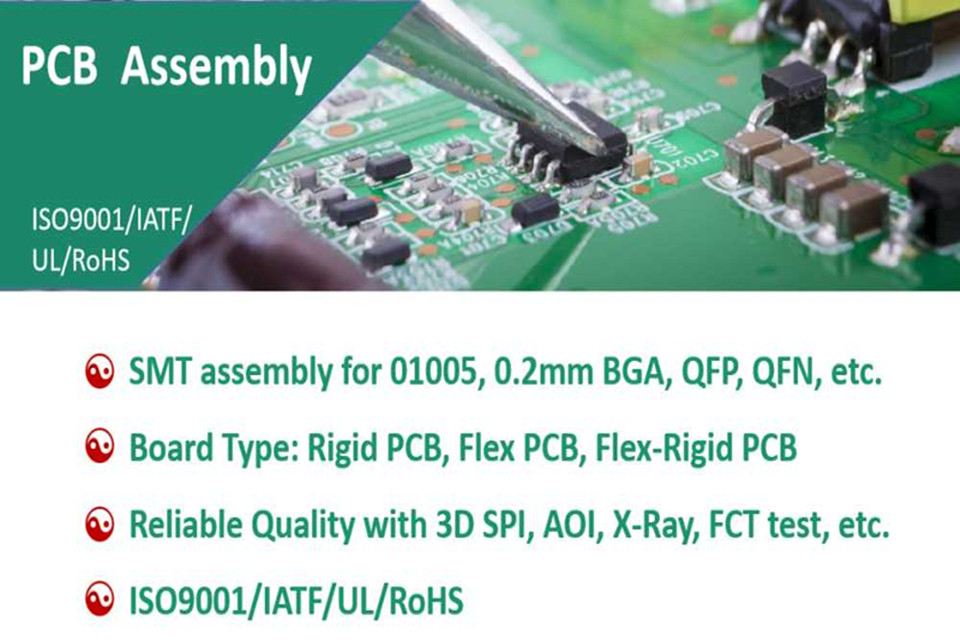
PCB Assembly
PCB Assembly
In the process of improving quality of modern life, electronic products as a key role and promote the innovation of various fields technical systems . The widespread application of cutting-edge technologies such as artificial intelligence (AI), wireless communication, machine learning and the Internet of Things (IoT) has injected strong momentum into the electronic equipment manufacturing industry. These smart devices have deeply penetrated into every subtle corner of human life, effectively responding to many social challenges and bridging the development gap. Especially when people look at the powerful functions of popular devices such as smartphones and computers, they are all impressed by their exquisite operating mechanisms. The core of these smart devices, the precision circuit board system, supports cutting-edge functions such as wireless communication, automatic control and multi-tasking through complex design architecture. At present, with the continuous breakthroughs in PCB assembly and manufacturing technology, the industry is accelerating the innovation and upgrading of printed circuit boards (PCBs) and their assembly processes (PCBA)
What is PCB Assembly?
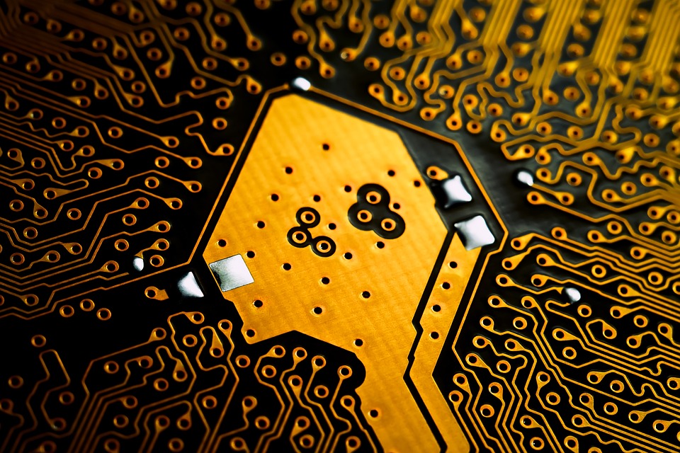
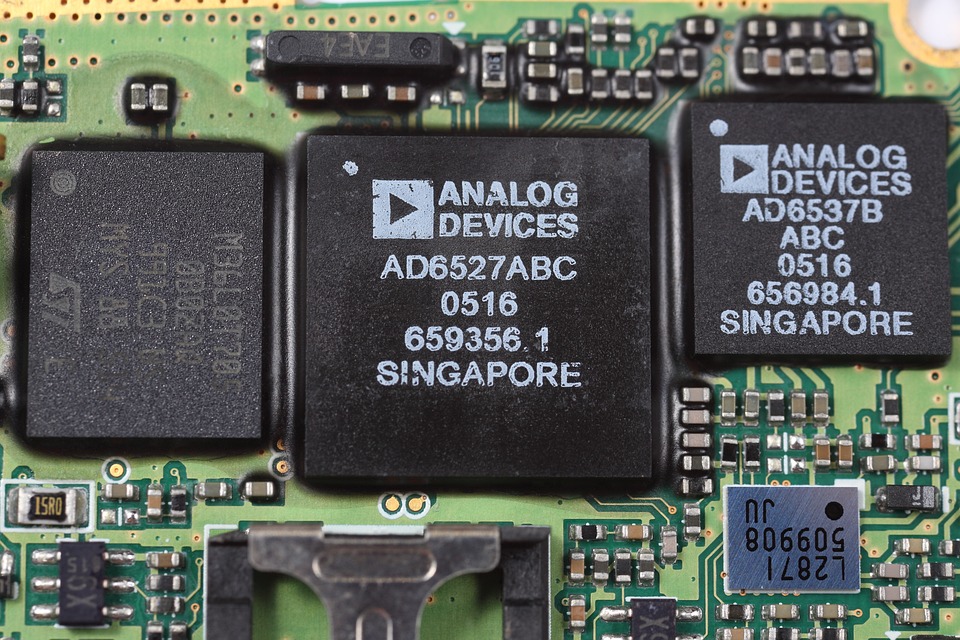
PCB assembly (Printed Circuit Board Assembly) is the key process of electronic manufacturing. It refers to electronic components such as resistors, capacitors, integrated circuits on a Bare PCB with a completed circuit design through a welding process to form an electronic module with complete functions. This process not only determines the functionality and reliability of electronic equipment, but is also a key step in quality control before mass production of products. The assembly of printed circuits can be done manually or by machine. The automated assembly of PC boards is assembled using automated equipment in most cases due to its high efficiency and good reliability. Generally speaking, there are three types of PCB board assembly: PTH assembly, SMT assembly, and mixed technology (SMT + through-hole)
What is main types of Printed Circuit Board Assembly?
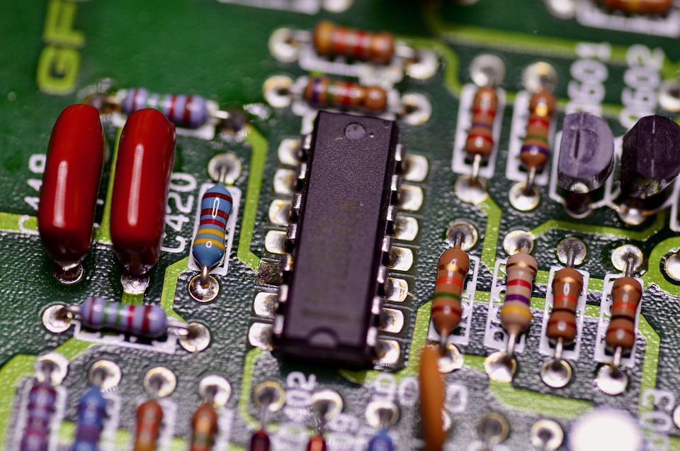
PTH Through Hole Technology
Key Features:
• Durable connections: Ideal for high-power components (transformers, connectors) using wave soldering with dual-peak technology.
• Thermal resilience: Withstands -40°C to 150°C environments for automotive/industrial use.
• Applications: Power supplies, industrial controllers
5 advantages of PTH through-hole technology:
Ultra-high mechanical strength and reliability 360° ring solder joint design, vibration resistance improved by 3 times, suitable for high-stress scenarios such as automotive electronics and military equipment.
High power and high current carrying capacity Support 10A-100A high current transmission, adapt to transformers and high-power capacitors, and meet the needs of power modules.
Tolerance to extreme environments Temperature range-55°C to 260°C, passed 1000 thermal cycle tests, in line with military and AEC-Q100 certification.
Low-cost maintenance and flexible iteration Components can be replaced by manual soldering, rework cost is 60% lower than SMT, suitable for customized medical equipment needs.
Mature process and fast delivery Compatible with single-layer to 20-layer PCBs, wave soldering yield> 99.5%, support 72-hour fast proofing.
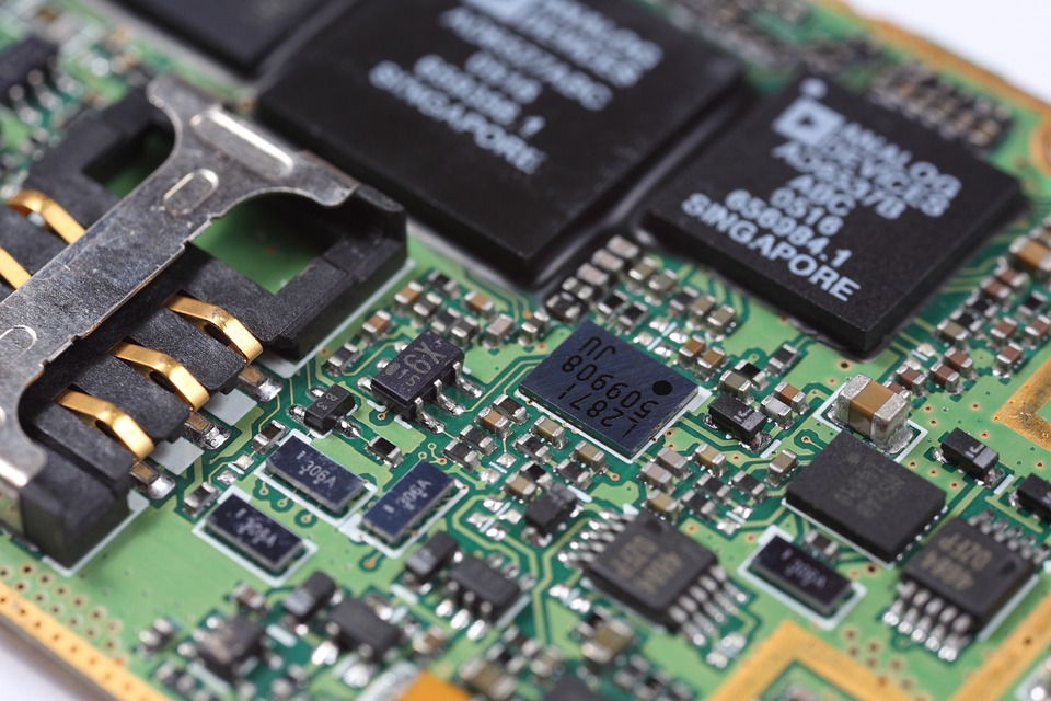
Surface Mount Technology
Features:
• Micro-component handling: Supports 01005 and 03015 packages for ultra-compact designs.
• Reflow soldering: Utilizes SAC305 or advanced Bi/Ni-doped alloys for lead-free, high-reliability joints (melting point: 235–240°C).
• Applications: Smartphones, wearables, IoT devices.
5 advantages of SMT technology
Ultra-high precision and miniaturized integration ±0.05mm mounting accuracy, supports 01005 components, PCB volume is reduced by 60%, and is suitable for high-density scenarios such as smart wearables and 5G communications.
Fully automated and efficient production 80,000 points/hour mounting speed, yield>99.9%, efficiency increased by 20 times, labor costs reduced by 50%.
High reliability and environmental compatibility Nitrogen reflow process (void rate <5%), passed IPC-A-610 Class 3 certification, lifetime over 10 years, RoHS compliant.
High-frequency performance and vibration resistance Short pin design reduces electromagnetic interference, high-frequency characteristics reach 3GHz, vibration resistance increased by 3 times, suitable for vehicle-mounted and industrial equipment.
Cost optimization and fast delivery Material waste is reduced by 30%, comprehensive cost is reduced by 50%, small batch customization is supported, 7-day fast proofing delivery.
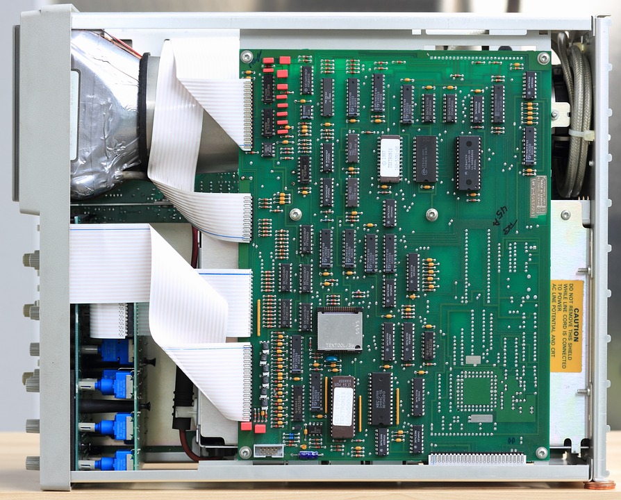
Mixed technology (SMT + thru-hole)
Features:
• Dual-sided integration: Combines SMT (top layer) with PTH robustness (bottom layer) for complex layouts.
• 3D-SPI/AXI inspection: Achieves 99% defect detection via AI-powered 3D solder paste inspection and X-ray test.
• Applications: Medical devices, Automotive ADAS systems.
5 advantages of Mixed technology (SMT + thru-hole)
High-density integrated design and flexible SMT+PTH is compatible with micro-chips and high-power through-hole components, saving PCB area by 30%, and is suitable for high-complexity scenarios such as automotive electronics.
Dual process complementarity improves reliability SMT precision mounting (±0.05mm) combined with PTH anti-vibration solder joints, passed IEC-60068 certification, and extended life by 50%.
Cost and performance dual-optimal solution Reduce PCB layer requirements (2→1 layer), reduce material costs by 20%, and support high-speed signal and high-current transmission.
Full-scenario environmental adaptability Temperature resistance -40°C to 150°C, passed AEC-Q100 (automotive) and ISO-13485 (medical) certification.
Efficient mixed-line production and fast delivery Automated SMT+selective wave soldering linkage, yield>99.8%, support 7-day fast proofing.