-
Xinxintian Industrial Zone, Shajing Street,Bao'an District, Shenzhen, China
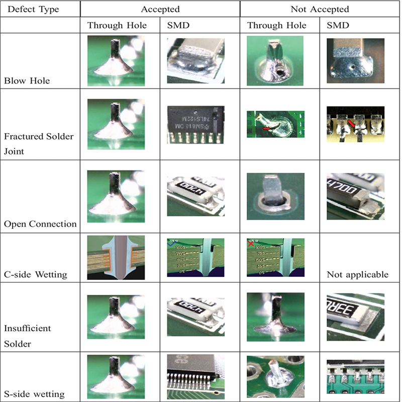
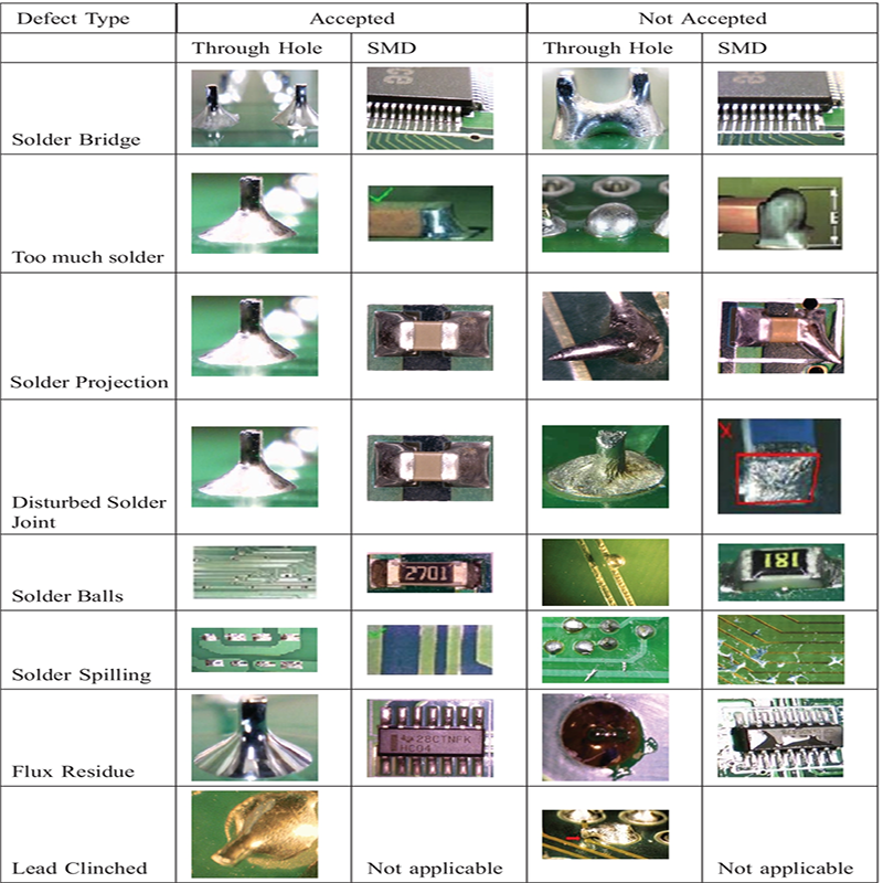
4 types poor SMT Assembly analysis
Full analysis of poor SMT welding: 4 types of defect causes and high-precision manufacturing solutions
Abstract: In the field of electronic manufacturing, SMT (surface mount technology) is the core process of PCBA foundry services, but up to 4 types of poor welding problems in its production process directly affect product quality and customer trust.
Based on industry authoritative standards (such as IPC-A-610) and the practices of leading global companies, this article systematically analyzes the causes of key defects such as empty soldering, bridging, and board explosion, and provides feasible process optimization solutions to help companies achieve yield improvement and cost reduction and efficiency improvement.
I. Welding quality defects: from micro solder joints to macro failures
1. Empty soldering and false soldering: hidden electrical killers
Performance: The solder joints are not combined, resulting in open circuits or abnormal signal transmission. Deep causes:
• Material defects: oxidation of pads and insufficient activity of solder paste (it is recommended to use a no-clean solder paste containing 3.0% activator).
• Process out of control: The heating rate of the reflow soldering preheating zone is greater than 3°C/s, causing the flux to volatilize prematurely. Solution:
• Precise control of solder paste printing: Use laser-cut steel mesh (tolerance ±15μm) and use SPI (solder paste detector) to monitor thickness in real time (target value 0.12-0.15mm).
• Temperature curve optimization: Set a three-stage reflow curve (preheating 120-150°C/90s, reflow 217-245°C/60s, cooling slope <4°C/s).
2. Bridging and cold soldering: dual challenges of high-density assembly
Typical case: The risk of bridging increases by 30% when the pin pitch of the QFP package is less than 0.4mm. Key technological breakthroughs:
• Steel mesh design: A trapezoidal opening design (width reduction of 5%) is used for fine-pitch components to reduce the amount of solder paste released.
• Nitrogen protection welding: Inject nitrogen (oxygen content <1000ppm) into the reflow furnace to reduce surface tension and inhibit solder bead splashing.
II. Abnormal component placement: the game between precision and reliability
1. Wrong parts and polarity reversal: blind spots in supply chain collaborative management
Data warning: Batch accidents caused by wrong parts account for 18% of SMT quality losses. Prevention and control system:
• Intelligent material traceability: Import the MES system and use QR code to achieve full traceability from BOM to placement.
• AOI (automatic optical inspection): Set up a dual-camera inspection station after placement to identify polarity identification and component silk screen (accuracy ±0.01mm).
2. Floating position: placement control from a dynamic perspective
Root cause: nozzle vacuum pressure fluctuation >10% or placement height error >0.05mm. Equipment upgrade path:
• High-precision placement machine: Use a flying focus vision system (such as Fuji NXT III) to achieve 15μm placement accuracy.
• Vibration suppression technology: Add an active damper to the high-speed placement head to reduce the offset caused by motion inertia.
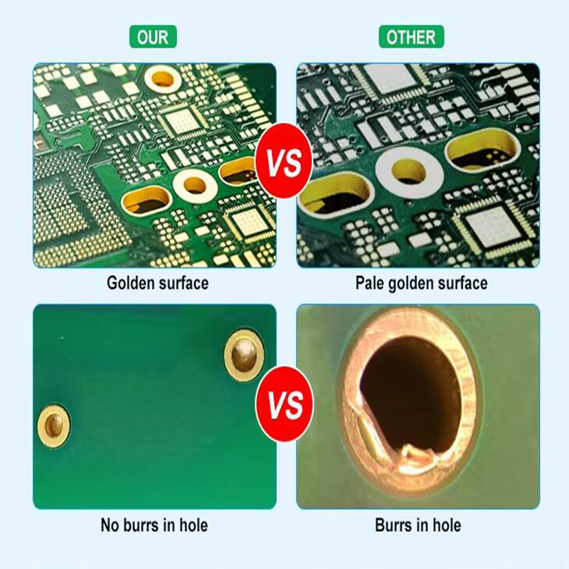
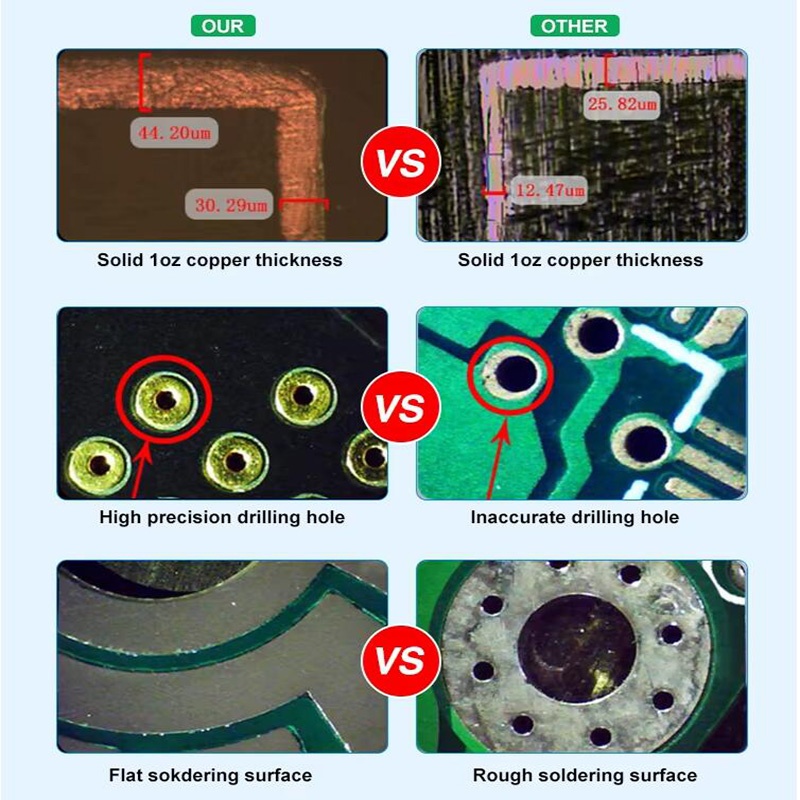
III. PCB damage and contamination: Collaborative innovation of materials science and technology
1. Explosion and warping: Engineering solution to thermodynamic failure
Material breakthrough:
• High-frequency board selection: Use TG170 halogen-free substrate, which improves temperature resistance by 40% (compared to traditional FR-4).
• Symmetrical stacking design: Implement copper foil balanced layout (tolerance ±5%) for PCBs with more than 8 layers to reduce the difference in Z-axis expansion coefficient.
2. Solder balls and foreign matter: the nano-level war of cleanliness control
Cleanroom standards:
• Particle control: meet ISO 14644-1 Class 7 standard (particles ≤352,000 per cubic meter > 0.5μm).
• Electrostatic protection: surface resistance of work surface 1×10^6-1×10^9Ω, humidity controlled at 40-60%RH.
IIII. Systematic quality engineering: full process control from DFM to SPC
1. Design-side prevention (DFM)
• Pad optimization: dog-bone pads are used for 0201 components to reduce the risk of tombstones.
• Heat sink design: heat dissipation vias are set around high-power devices (aperture 0.3mm, spacing 1mm).
2. Manufacturing monitoring (SPC)
• Key parameter control: Set Xbar-R control charts (CPK≥1.33) for solder paste thickness, reflow peak temperature, etc.
• AI defect prediction: Analyze historical data based on deep learning algorithms to warn of cold soldering and false soldering trends in advance.
Summary and action guide
SMT welding quality is the result of four-dimensional coordination of materials, equipment, process, and management. Enterprises need to establish a quality system covering the entire life cycle of products. The specific paths include:
- Technology upgrade: Introduce intelligent inspection equipment such as 3D SPI and AOI (refer to Koh Young solution).
- Standard implementation: Implement IPC-7711 rework standards and J-STD-001 welding requirements.
- Ecological synergy: Jointly develop customized materials with solder paste suppliers (such as Alpha Metals).
Contact our team of SMT process experts now to obtain the “High-Density PCB Assembly White Paper” and free production line diagnosis services, and work together to create a new benchmark for zero-defect electronic manufacturing!