¿Qué es el AOI en PCB y SMT?
Abstracto
En el procesamiento de parches SMT, AOI (Inspección óptica automática) Es el eslabón fundamental para garantizar la calidad del producto. Este artículo analizará en profundidad el principio de funcionamiento, el proceso de inspección, las principales ventajas y diferencias entre la prueba AOI y la SPI (inspección de pasta de soldadura), y combinará casos y datos de la industria para ayudar a los lectores a comprender plenamente su papel clave en la fabricación electrónica y ofrecer sugerencias de soluciones viables.
Tabla de contenido
I. El principio fundamental de AOI (Inspección óptica automática)
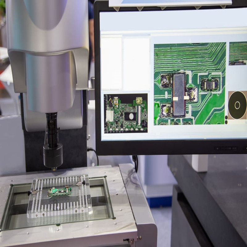
Prueba AOI (Inspección Óptica Automática) escanea la superficie de la placa PCB a través de una cámara CCD de alta definición, recopila imágenes y las compara con parámetros calificados en la base de datos para identificar juntas de soldadura, montaje de componentes y defectos de proceso.
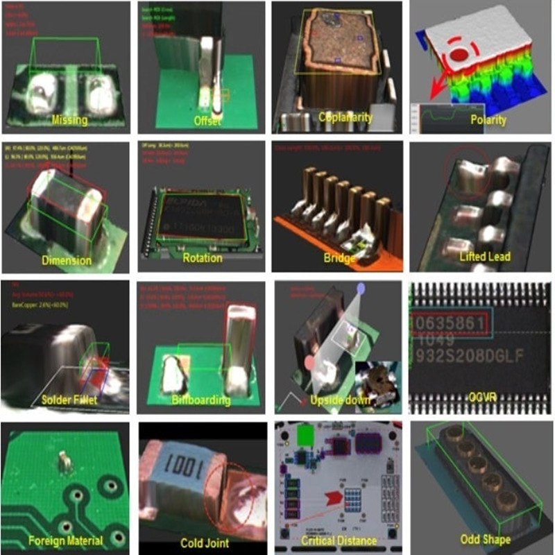
Contenido de la inspección
- Defectos de componentes: piezas faltantes, polaridad incorrecta, desplazamiento, montaje inverso y efecto lápida.
- Defectos de soldadura: cortocircuito, soldadura vacía, soldadura virtual, bolas de soldadura y perlas de soldadura.
- Problemas de proceso:impresión desigual de pasta de soldadura, contaminación por materias extrañas y tamaño anormal de los componentes.
II. Proceso completo de AOI (Inspección óptica automática)
- Adquisición de imágenes
- La placa PCB ingresa al equipo a través de la cinta transportadora y la cámara de alta definición escanea la superficie para obtener datos de imagen de los componentes y las uniones de soldadura.
- Aspectos técnicos destacados:Admite imágenes 2D/3D y se adapta a placas HDI de alta densidad y PCB de gran tamaño.
- Comparación de parámetros
- Los datos de la imagen se comparan con la biblioteca de parámetros calificados preestablecidos para identificar anomalías como desplazamiento y cortocircuito.
- algoritmo de IA:El modelo de aprendizaje profundo optimiza continuamente la tasa de falsas alarmas y la tasa de precisión del reconocimiento de defectos complejos supera 99%.
- Marcado de defectos y retroalimentación
- Marque la ubicación del defecto a través de la pantalla o el sistema de marcado automático y envíe retroalimentación a la estación de mantenimiento en tiempo real.
- Control de bucle cerrado:Las estadísticas de datos de defectos generan informes SPC para ayudar a mejorar el proceso.
III. Ventajas principales de AOI (Inspección óptica automática)
1. Reemplazo de alta precisión para la inspección visual manual.
- Resolución de 0,01 mm, eliminando errores humanos y mejorando la consistencia de la detección en más de 90%.
- Adaptabilidad ambiental:No se ve afectado por la luz ni la temperatura, lo que garantiza un funcionamiento estable durante todo el día.
2. Control de bucle cerrado en tiempo real
- Respuesta en milisegundos, tasa de intercepción de defectos de hasta 99,5%, evitando que los productos defectuosos se transfieran a procesos posteriores.
- Basado en datos:Genere estadísticas de clasificación de defectos, optimice los procesos de producción y aumente el rendimiento mediante 3%-8%.
3. Adaptabilidad a todos los escenarios
- Cobertura multisectorial:Ampliamente utilizado en electrónica automotriz, nuevas energías y electrónica de consumo.
- Compatibilidad:Admite requisitos de inspección complejos desde microcomponentes 0201 hasta empaquetado BGA.
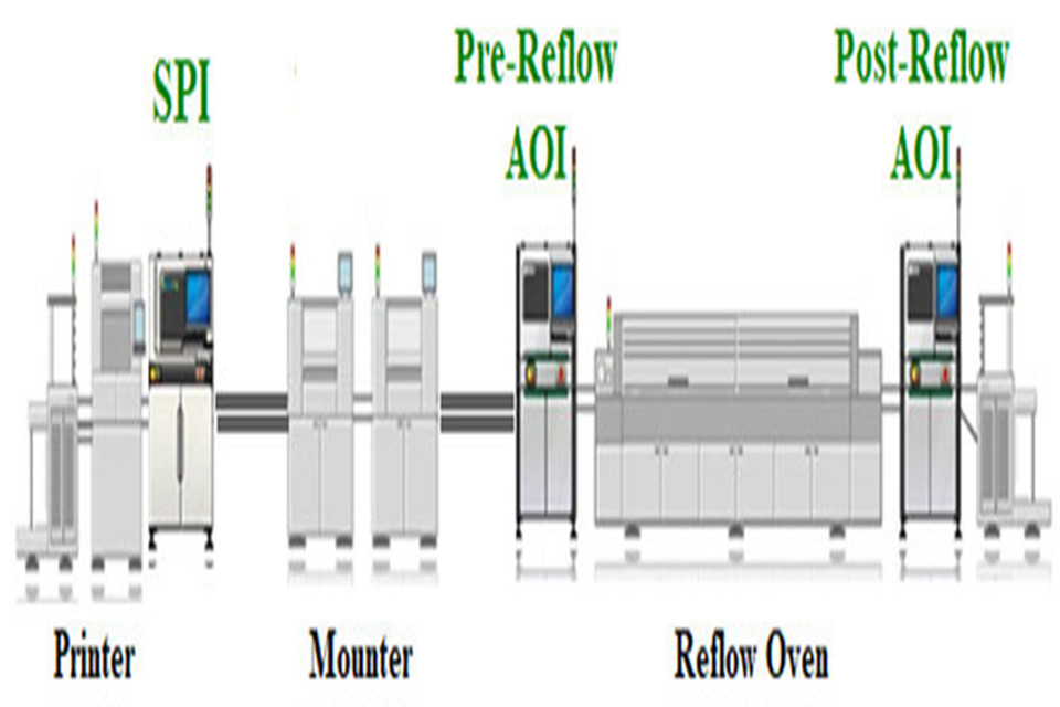
En cuarto lugar, la diferencia entre AOI y SPI: ¿Cómo elegir una solución de inspección adecuada?
| Dimensiones de comparación | AOI (Inspección óptica automatizada) | SPI (Inspección de pasta de soldadura) |
|---|---|---|
| Fase de inspección | Inspección posterior al parche/post soldadura | Inspección posterior a la impresión de pasta de soldadura |
| Objetivo principal | Identificar la colocación de componentes y defectos de soldadura. | Evaluar la calidad de impresión de la pasta de soldadura |
| Defectos típicos | Desplazamiento, cortocircuito, lápida, fuga de soldadura | Espesor desigual de la pasta de soldadura, impresión offset, desconexión |
| Enfoque técnico | Procesamiento de imágenes 2D/3D | Escaneo láser 3D + Imágenes multiespectrales |
Recomendaciones de la industria:La combinación de AOI + SPI puede lograr un monitoreo de calidad de proceso completo de las líneas de producción SMT, y la tasa de detección de defectos se puede incrementar en 80%.
Cinco. Preguntas frecuentes: Respuestas a las preguntas frecuentes de los clientes
¿Qué tan precisa es la inspección AOI?
Utilizando una lente de resolución de 0,01 mm y combinado con algoritmos de IA, la tasa de precisión de reconocimiento de defectos supera el 99%.
¿Qué tipos de defectos puede detectar la AOI?
Incluyendo desplazamiento de componentes, cortocircuito, unión de soldadura vacía, unión de soldadura con fugas, error de polaridad, etc.
What are the advantages of AOI compared with manual visual inspection?
Elimina errores humanos, aumenta la velocidad de detección 5 veces y apoya el análisis de datos.
What industries is AOI suitable for?
Ampliamente utilizado en electrónica automotriz, nuevas energías, electrónica de consumo y otros campos.
¿Cuál es el costo de la inspección AOI?
La inversión inicial es alta, pero al reducir los costos de mantenimiento y las tasas de descarte, el costo se puede recuperar en 6 meses.
¿Cómo elegir un proveedor de equipos AOI?
Dar prioridad a los fabricantes que ofrezcan soluciones personalizadas, soporte técnico y garantías postventa.
Resumen
Inspección óptica AOI Es una herramienta indispensable de inspección de calidad en el procesamiento de parches SMT. Su alta precisión, eficiencia y funciones inteligentes están transformando la industria de fabricación electrónica. Al combinar imágenes 3D, algoritmos de IA y análisis de datos, AOI no solo mejora la calidad del producto y el rendimiento, sino que también proporciona competitividad esencial a las empresas para reducir costos y aumentar la eficiencia.