-
Xinxintian Industrial Zone, Shajing Street,Bao'an District, Shenzhen, China
The Importance of SMT Solder Masking in High-Density PCB Manufacturing
[ad_1]
The Importance of SMT Solder Masking in High-Density PCB Manufacturing
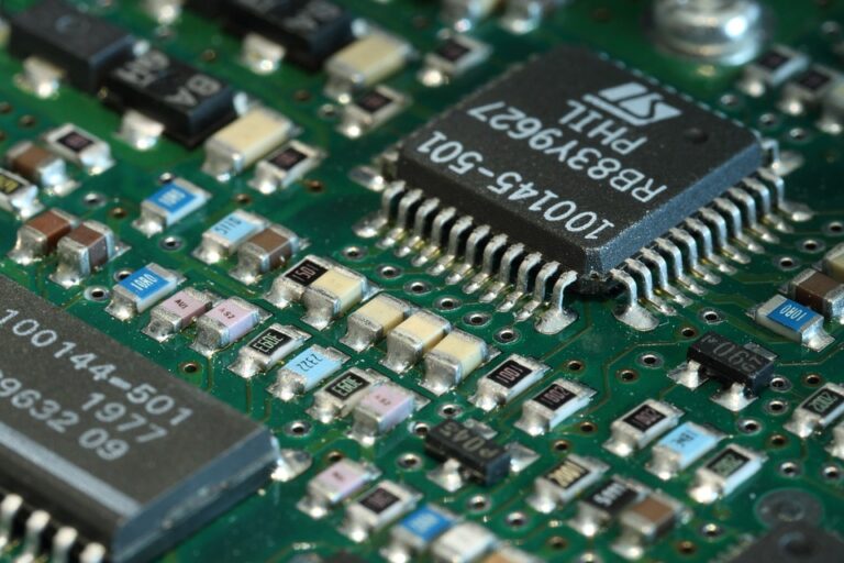
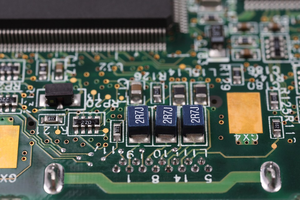
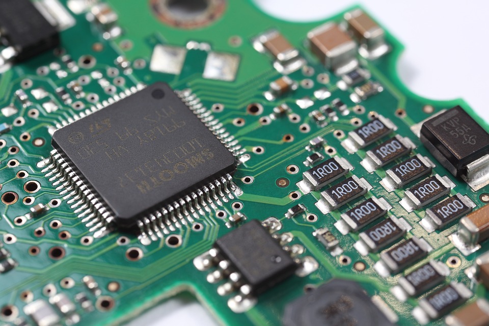
SMT (Surface Mount Technology) solder masking is a crucial step in the manufacturing process of high-density printed circuit boards (PCBs). It plays a vital role in ensuring the quality and reliability of the final product. In this article, we will explore the importance of SMT solder masking in high-density PCB manufacturing and its impact on the overall performance of the PCB.
What is SMT Solder Masking?
SMT solder masking is a process that involves applying a thin layer of photoresist material to the surface of the PCB. This layer is then exposed to ultraviolet (UV) light through a mask, which creates a pattern of openings in the photoresist material. The areas that are not exposed to UV light remain covered with the photoresist material, creating a “mask” that prevents solder from flowing into unwanted areas of the PCB.
Why is SMT Solder Masking Important?
SMT solder masking is important for several reasons:
- Prevents Solder Bridging**: SMT solder masking prevents solder from flowing between adjacent pads or components, which can cause short circuits and render the PCB unusable.
- Improves Component Placement**: SMT solder masking ensures that components are placed accurately and precisely on the PCB, reducing the risk of misalignment and increasing the overall reliability of the PCB.
- Enhances Solder Joint Quality**: SMT solder masking helps to create a strong and reliable solder joint by preventing solder from flowing into unwanted areas and reducing the risk of solder balls or bridges.
- Reduces Manufacturing Defects**: SMT solder masking helps to reduce manufacturing defects by preventing solder from flowing into unwanted areas and reducing the risk of component damage during the manufacturing process.
Impact of SMT Solder Masking on High-Density PCB Manufacturing
The importance of SMT solder masking is particularly critical in high-density PCB manufacturing, where the density of components and the complexity of the design can make it difficult to achieve accurate and reliable solder joints. SMT solder masking helps to ensure that the PCB is manufactured with precision and accuracy, even in the most complex designs.
In high-density PCB manufacturing, SMT solder masking is used to:
- Prevent Solder Filling**: SMT solder masking prevents solder from filling in the gaps between adjacent components, which can cause short circuits and render the PCB unusable.
- Improve Component Density**: SMT solder masking allows for higher component density by preventing solder from flowing into unwanted areas and reducing the risk of component damage during the manufacturing process.
- Enhance Solder Joint Reliability**: SMT solder masking helps to create a strong and reliable solder joint by preventing solder from flowing into unwanted areas and reducing the risk of solder balls or bridges.
Conclusion
In conclusion, SMT solder masking is a critical step in the manufacturing process of high-density PCBs. It plays a vital role in ensuring the quality and reliability of the final product by preventing solder bridging, improving component placement, enhancing solder joint quality, and reducing manufacturing defects. The importance of SMT solder masking is particularly critical in high-density PCB manufacturing, where the density of components and the complexity of the design can make it difficult to achieve accurate and reliable solder joints.
FAQs
Q: What is the purpose of SMT solder masking?
A: The purpose of SMT solder masking is to prevent solder from flowing into unwanted areas of the PCB, ensuring accurate and reliable solder joints.
Q: Why is SMT solder masking important in high-density PCB manufacturing?
A: SMT solder masking is important in high-density PCB manufacturing because it helps to prevent solder bridging, improve component placement, enhance solder joint quality, and reduce manufacturing defects.
Q: What are the benefits of SMT solder masking?
A: The benefits of SMT solder masking include improved component placement, enhanced solder joint quality, reduced manufacturing defects, and improved overall reliability of the PCB.
Q: How is SMT solder masking applied?
A: SMT solder masking is applied by applying a thin layer of photoresist material to the surface of the PCB, exposing it to UV light through a mask, and then developing the photoresist material to create a pattern of openings.
Q: What are the common defects that can occur without SMT solder masking?
A: Common defects that can occur without SMT solder masking include solder bridging, component misalignment, and poor solder joint quality.
[ad_2]

admin
You may also like
PCB Assembly Design for Manufacturing (DFM): A Guide to Making it Right the First Time
SMT vs. thru-Hole: The Pro and Cons of Each PCB Assembly Technique