¿Nuevos consejos para el diseño de ensamblaje de PCB en 2025?
Abstracto
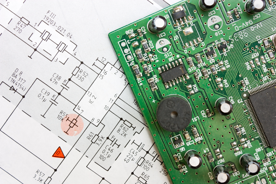
pcb assembly design is the procedure of planning and specifying cómo digital components will be put and soldered onto a Printed Circuit Board (PCB) to create a functional electronic circuit.
Consider it this way:
- A bare PCB resembles a city map with empty whole lots and roadways drawn on it.
- pcb assembly design is the comprehensive building and construction prepare for that city, deciding which buildings (elements) take place which whole lots, how they should be oriented, and what machinery and procedures are needed to build the entire city successfully and reliably.
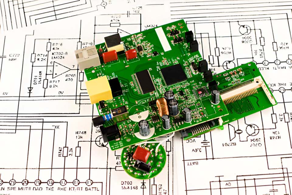
The final, inhabited board is called a PCBA (Printed Circuit Board Assembly).
Tabla de contenido
¿Qué implica el diseño del ensamblaje de PCB?
PCB Assembly Layout is not a solitary step however an all natural procedure that links the void in between an academic circuit layout and a physical, manufacturable item. It involves several crucial stages and considerations:
1. Estilo esquemático
This is the logical plan. It’s a layout that reveals all the components (resistors, capacitors, integrated circuits, and so on) and just how they are electrically attached to each other making use of symbols.
- It answers: “What needs to be linked to what?”
- It does NOT response: “Where will these parts literally take place the board?”
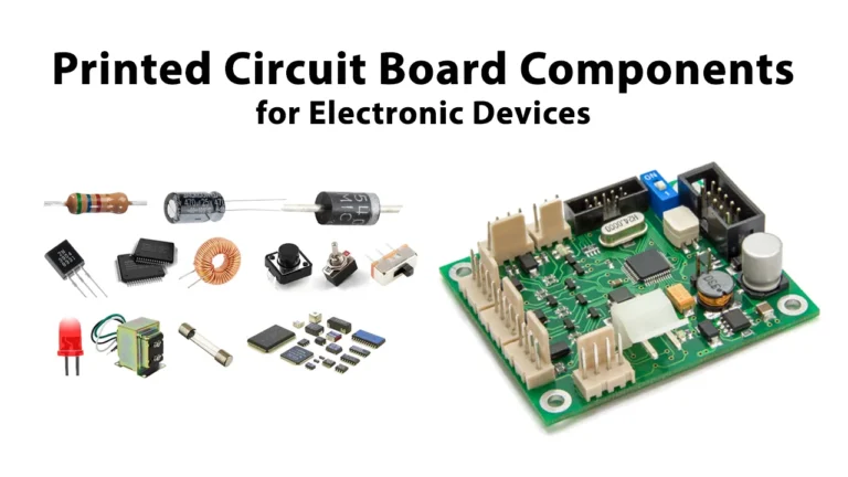
2. Opción de componente y gasto de materiales (BOM).
This is the “shopping list” for the circuit. For every component in the schematic, the designer chooses a specific physical component. This includes picking:.
- Plan Kind: E.g., a small surface-mount 0402 resistor vs. a huge through-hole resistor.
- Manufacturer and Part Number: Ensures the appropriate part with the ideal requirements is bought.
- Impact: The physical pattern of pads on the PCB that the component will certainly be soldered to.
The BOM is a critical record for purchasing and production.
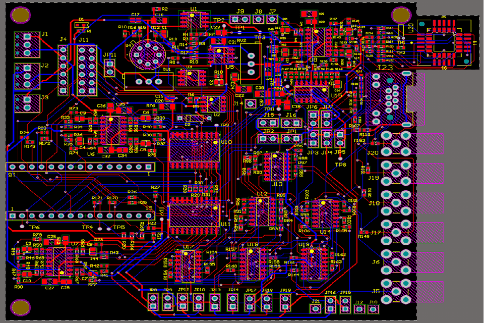
3. Formato PCB.
This is where the schematic is converted right into a physical layout. Utilizing specific software program (like Altium Developer, KiCad, or Eagle), the developer:.
- Defines the Board Shape and Size: The physical measurements of the PCB.
- Places Elements: Sets up the physical components on the board. This is an important action in setting up style.
- Routes Traces: Attracts the copper “cords” (traces) that link the elements according to the schematic.
4. Style for “X” (DFX).
This is the core of great setting up style. It indicates designing with completion objective in mind. One of the most crucial facets are:.
- Style for Manufacturability (DFM): Makes sure the style can be created accurately and with a high yield.
- Example: Are the copper traces and the rooms in between them wide enough for the producer’s tools to develop them without errors?
- Style for Assembly (DFA): Makes certain the elements can be quickly and instantly put and soldered onto the board. This is vital for automation.
- Example: Are components spaced much sufficient apart so the pick-and-place device’s nozzle can put them without encountering nearby parts? Are all comparable elements oriented parallel to lessen equipment head rotation?
- Layout for Test (DFT): Makes sure the last constructed board can be examined to confirm it works correctly.
- Instancia: Are there specific “test factors” included on the board where probes can determine voltages to detect issues?
Consideraciones sobre trucos en el diseño del ensamblaje de PCB.
A developer must assume like an assembly line robot. Here are the functional details they concentrate on:.
- Element Positioning: .
- Clearance: Keeping adequate room in between components.
- Orientation: Straightening components (particularly polarized ones like diodes and some capacitors) correctly. Grouping similar parts aids quicken computerized setting up.
- Gestión térmica: Positioning heat-generating parts where they can dissipate warm efficiently, frequently far from heat-sensitive components.
- Tailing: Staying clear of putting little components behind high ones, which can trigger soldering problems during the reflow process.
- Assembly Modern technology: .
- Surface-Mount Technology (SMT): Parts are placed directly externally of the board. This is utilized for the majority of contemporary electronics because of its tiny dimension and viability for automation.
- Tecnología de orificio pasante (THT): Components have leads that go through openings in the board and are soldered on the other side. This is used for components that require strong mechanical links, like big adapters or capacitors. Many boards make use of a mix of both.
- Panelización: .
- For automation, multiple copies of a solitary PCB are commonly manufactured on a larger board called a “panel.” The design must include attributes (like V-grooves or mouse attacks) that permit the specific boards to be quickly and cleanly separated after setting up.
- Fiducial Marks: .
- These are little copper circles or patterns positioned on the PCB. Automated pick-and-place makers make use of cams to find these fiducials as specific referral factors, ensuring every element is put with severe precision.
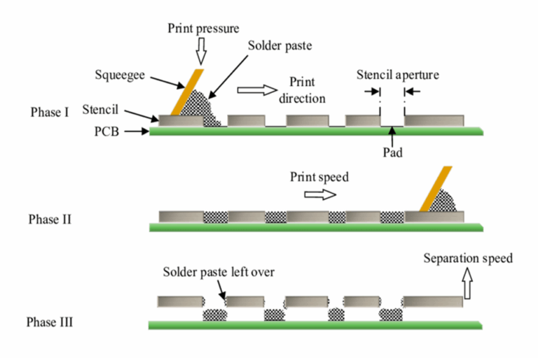
- Solder Mask and Solder Paste: .
- Solder Mask: The eco-friendly (or various other color) layer on a PCB. It avoids solder from mistakenly bridging between 2 pads, which would certainly trigger a short circuit.
- Solder Paste Stencil: The setting up style generates an apply for developing a thin metal stencil. This pattern is laid over the bare PCB, and solder paste is squeegeed with the openings, depositing it completely on the pads where components will be placed.
- Silkscreen: .
- This is the human-readable text and icons printed on the board (usually in white). It consists of element designators (R1, C1, U1), polarity marks, and business logos. It’s vital for manual assembly, screening, and repair.
¿Por qué es tan importante el diseño del ensamblaje de PCB?
- Functionality: A bad layout can result in a circuit that does not operate at all.
- Reliability: A great layout guarantees the item will certainly work constantly over its lifetime, even under tension.
- Expense: Smart assembly layout selections (e.g., using typical parts, making for automation) can considerably reduce producing costs.
- Time-to-Market: A layout that is simple to make and examine can be generated much faster, obtaining the product to market in advance of the competition.
Preguntas Comunes Sobre SMD vs THT en la Configuración de PCB
What are the main differences in between SMD and THT in PCB setting up ?
La principal distinción entre SMD (Herramienta de Montaje Superficial) y THT (Tecnología Through-Hole) en la configuración de PCB depende de cómo se adjuntan las piezas a la placa. Las piezas SMD se sueldan directamente sobre la superficie de la PCB, mientras que los elementos THT tienen cables que se insertan a través de aberturas perforadas en la placa y luego se sueldan en el lado opuesto.
How do SMD and THT influence PCB design and production prices ?
SMD (Surface Area Mount Gadget) and THT (Through-Hole Innovation) considerably affect PCB design and manufacturing prices. SMD styles normally cause decrease production costs because of automated assembly, smaller sized component sizes, and increased board density. THT styles, while in some cases supplying benefits for high-power or high-reliability applications, can be extra expensive as a result of hand-operated setting up and larger element sizes.
¿Qué innovación ofrece una mejor integridad para las placas de semiconductores de alto rendimiento?
To ensure better integrity en high-performance semiconductor boards, several innovations may be involved, but the most effective innovation generally depends on the type of integrity you’re targeting
¿Cuáles son las consideraciones esenciales para elegir SMD o THT en el desarrollo de un producto nuevo?
Comparison Based on Assembly Process, Cost, Performance and Reliability
¿Cómo afecta el tamaño de los componentes a la opción de innovación en el ensamblaje de PCB?
Component dimension substantially impacts PCB setting up advancement by driving the fostering of miniaturization innovations like surface area mount innovation (SMT) and influencing the complexity of assembly processes. Smaller sized components allow for higher thickness PCB styles, allowing even more functionality in smaller sized tools and driving technology in locations like 5G and AI. This additionally brings about set you back financial savings because of reduced material use and the capacity for automated assembly.
¿Cuáles son las mejores técnicas para probar y confirmar la configuración de PCB utilizando SMD o THT?
To make sure top quality and integrity of PCBs making use of Surface Mount Modern technology (SMT) and Through-Hole Technology (THT), a number of screening methods are important. These include visual assessment, solderability testing, electric screening (such as in-circuit screening and flying probe testing), automated optical assessment (AOI), and practical testing.
Resumen
pcb assembly design is the art and science of turning a digital idea right into a physical, practical, and manufacturable item. It’s a crucial discipline that straight affects the cost, top quality, and success of virtually every digital tool in the. globe.