-
Xinxintian Industrial Zone, Shajing Street,Bao'an District, Shenzhen, China
From Gerber Files to PCB: A Step-by-Step Guide to PCBA Manufacturing Process
[ad_1]
Gerber files are a crucial step in the Printed Circuit Board Assembly (PCBA) manufacturing process. These files are used to guide the creation of the PCB, which is the backbone of modern electronics. In this article, we will take a step-by-step look at the PCBA manufacturing process, from Gerber files to the final product.
Step 1: Design and Design File Creation
The journey begins with the design of the PCB. This involves creating detailed designs using computer-aided design (CAD) software, such as Altium or KiCad. The design should include all the required components, such as components, tracks, and pads. The design is then saved as a gerber file, which is a standardized format for electronic design interchange.

Step 2: Gerber File Preparation
Once the design is complete, the gerber file is created. Gerber files are a critical step in the PCBA manufacturing process, as they contain all the necessary information for fabricating the PCB. The file includes the following details:
- Component placement and pin assignment
- Track geometry (width, spacing, and length)
- Pads and via information
- Layer stack-up and drill sizes
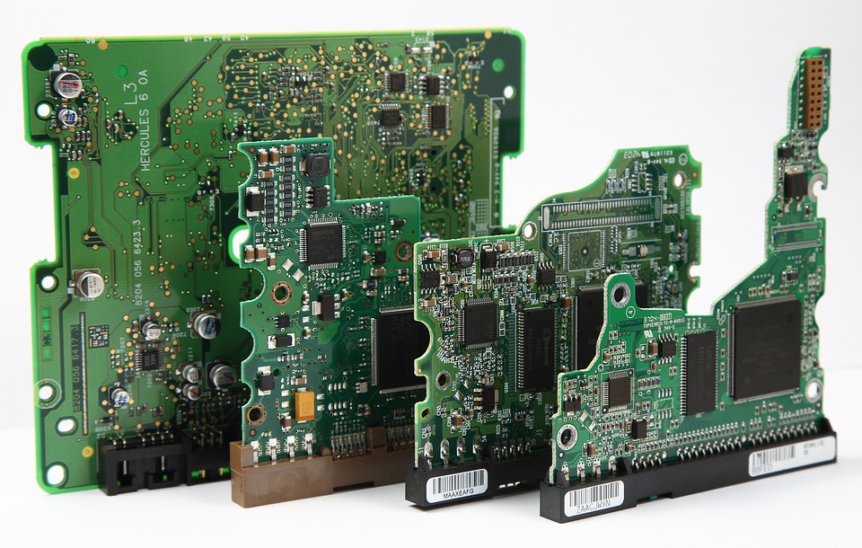
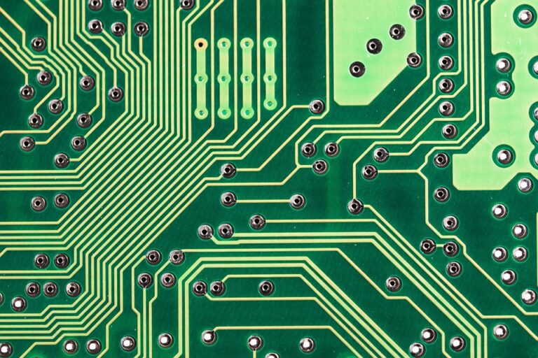
Step 3: PCB Fabrication
With the gerber file in hand, the PCB fabrication process begins. This step involves creating the physical circuit board using the information contained in the gerber file. The process typically includes:
- Photoplanes: Up to six layers are created using photoreduction techniques and photomasks.
- Solder mask application: A layer of solder mask is applied to prevent oxidation and improve soldering.
- Silk screening: Additional information, such as component names and numbers, is silk-screened onto the PCB.
- Drilling: Holes are drilled for components and through-hole soldering.
- Metallization: Copper traces and pads are created using a chemical etching process.

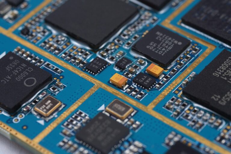
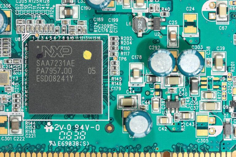
Step 4: Surface Mount (SMT) Assembly
After fabrication, the PCB is ready for surface mount (SMT) assembly. This step involves mounting components onto the PCB using automated placement equipment. The process includes:
- Component sorting and inspection
- Solder paste application
- Placement of components onto the PCB
- Solder reflow

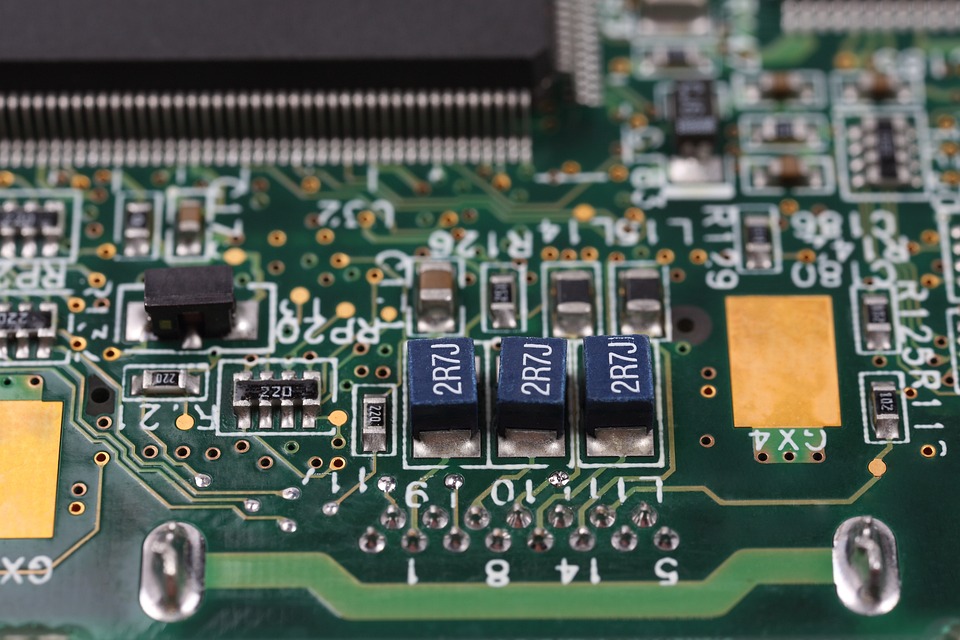
Step 5: Through-Hole Assembly (THA)
For components that require through-hole soldering, such as axial capacitors or resistors, THA is performed. This step involves:
- Component placement through the holes
- Solder reflow
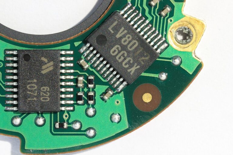
Step 6: Final Assembly and Testing
With all components in place, the PCB is now ready for final assembly and testing. This step includes:
- Component inspection
- Functional testing
- Visual inspection for defects
Conclusion
In conclusion, the PCBA manufacturing process involves several steps, from design and gerber file creation to final assembly and testing. Understanding these steps is crucial for ensuring the efficient and cost-effective creation of high-quality printed circuit boards. Whether you’re a designer, engineer, or manufacturer, this step-by-step guide has provided valuable insight into the PCBA manufacturing process.
FAQs
Q: What is a gerber file?
A: A gerber file is a standardized format for electronic design interchange, used to guide the creation of printed circuit boards.
Q: What is the difference between SMT and THA?
A: SMT (Surface Mount Technology) refers to the assembly of components onto the PCB using automated placement equipment, while THA (Through-Hole Assembly) involves assembling components through holes in the PCB.
Q: What is solder mask?
A: Solder mask is a layer applied to the PCB to prevent oxidation and improve soldering.
[ad_2]

admin
You may also like
PCB Repair and Troubleshooting: A Comprehensive Guide to Diagnosing and Fixing Common Issues – Tips and techniques for identifying and resolving common problems with PCBs.
Design for Testability (DFT) in PCBs: Maximizing Testability and Minimizing Debugging Time
A Guide to Choosing the Right PCB Assembly Company for Your Business