-
Xinxintian Industrial Zone, Shajing Street,Bao'an District, Shenzhen, China
Fixing Common PCB Design Issues: Tips and Tricks for Debugging Your Design
[ad_1]
Introduction
Designing a Printed Circuit Board (PCB) can be a complex and challenging task, requiring a combination of technical expertise, creativity, and attention to detail. Even with the best plans in place, mistakes can occur, and debugging becomes a necessary part of the process. In this article, we will discuss common PCB design issues, their causes, and the necessary steps to fix them, providing you with the skills and knowledge to overcome these challenges.
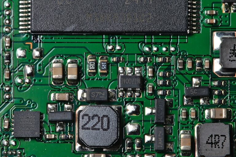
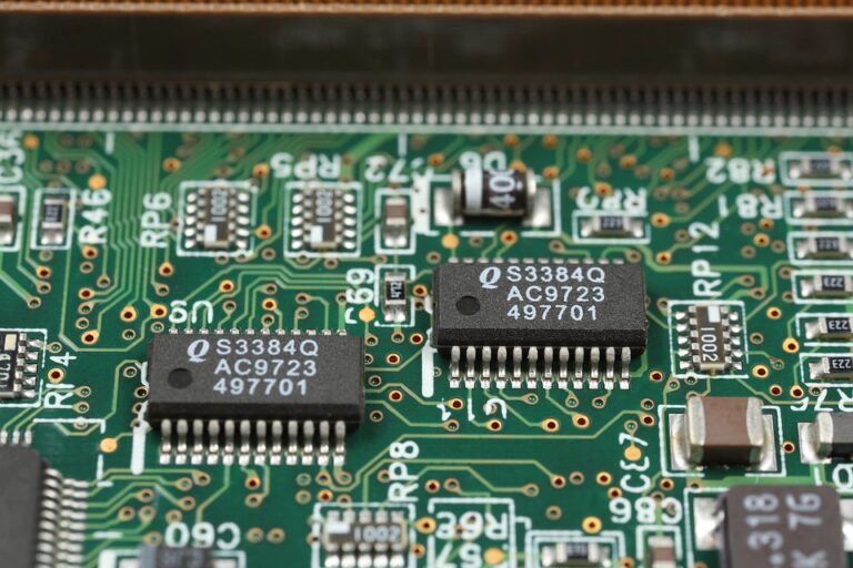
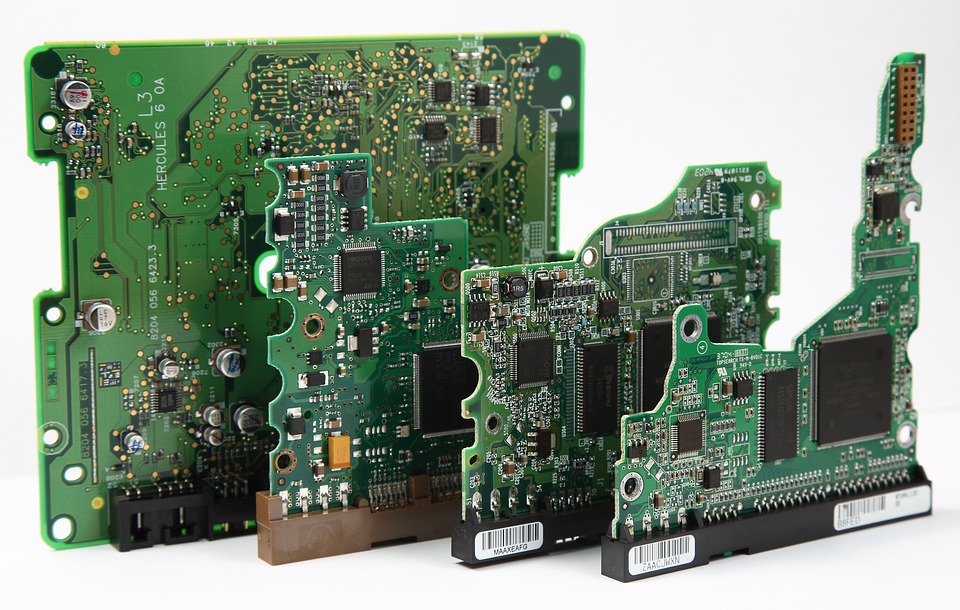
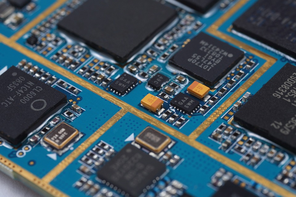
The Most Common PCB Design Issues
PCB design issues can be categorized into two main types: design and layout-related problems, and manufacturing-related issues. Some of the most common design-related issues include:
- Trap geysers: Also known as antipaths, these are unwanted paths of connectivity that can lead to signal integrity issues and even damage the PCB.
- Over-etching: This occurs when the etching process overreaches and removes too much of the resist material, resulting in a weak, fragile, and unreliable board.
- Inadequate solder mask application: A poorly applied solder mask can lead to poor solder joints and corrosion.
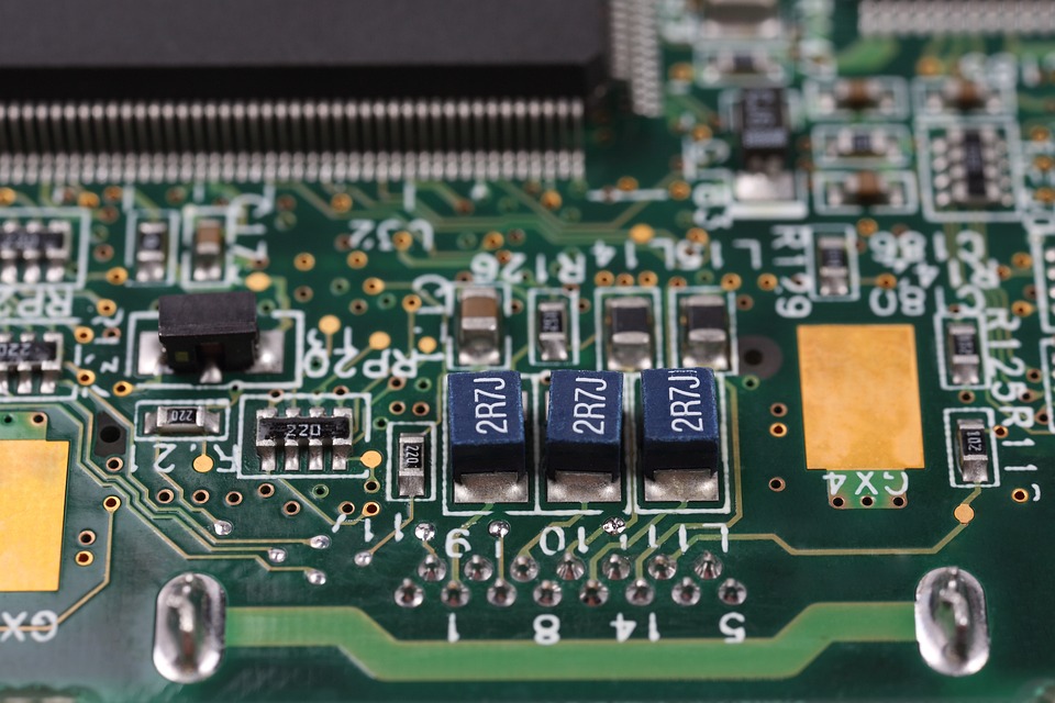
- Insufficient clearance between components: Leaving insufficient space between components can cause mechanical stress and interference, leading to board failure.
- Poor pinout planning: Incorrectly assigning pins or pins that are too close together can result in signal integrity issues, noise, and reduced reliability.
- Signal integrity issues: Issues like resulted impedance mismatch, signal degradation, and/Crosstalk can cause data corruption, errors, or signal loss.
- Resistance and inductance: Improper design can lead to excessive resistance and inductance, causing signal noise, and data loss.
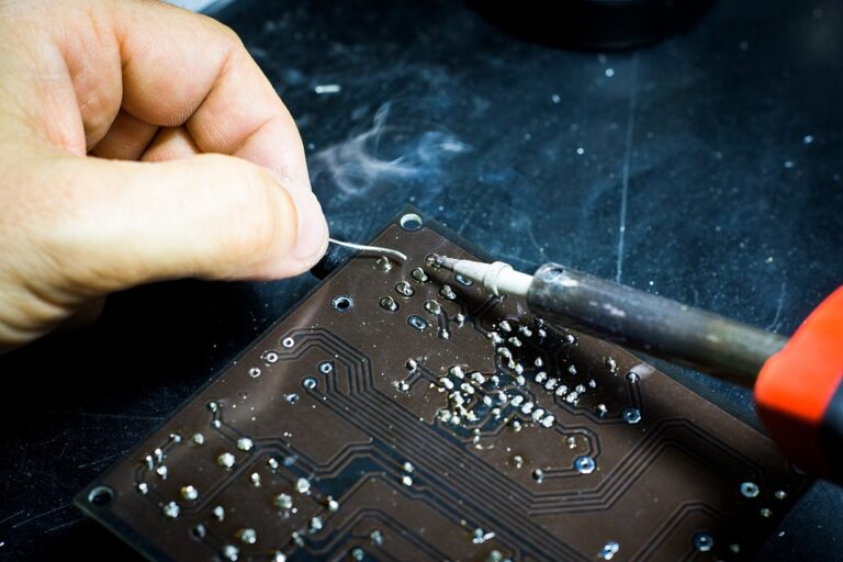
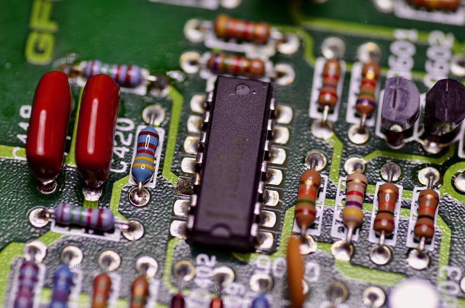
- Soldering issues: Poor soldering techniques, inadequate flux, or insufficient exposure can result in weak or brittle connections.
- Jumper wire crowding: Clustering jumper wires can cause electrical noise, reduced signal integrity, and increased temperatures, leading to component failure.
- Poor layer planning: Inadequate planning can lead to excessive layers, poor signal integrity, and increased production costs.
- Material selection: Inadequate material selection can result in a PCB that does not meet the required specifications, leading to functional issues or even board failure.
Manufacturing-related issues may include wrong component placement, polarity, and orientation, board warpage, and material defects.
Debugging Strategies
To effectively debug PCB design issues, follow these steps:
- Double-check the design for errors and inconsistencies, ensuring that the design meets specifications and is free from errors.
- Use design-for-debugging techniques, such as:
* Installing test pads for probing and testing
* Implementing debugging test points
* Adding sections for future modifications
* Using printk to add debug information - Use simulation software to analyze signal integrity and electromagnet compatibility (EMC) issues
- Use PCB design software features:
* Automatic repair
* Error detection
* Netlist generation
* Europecapping
* Pin assignment
* Component placement
* BOM management - Use prototype and testing fixtures to verify the design
- Monitor signals using a signal analyzer or oscilloscope
- Prioritize and segregate critical components and signal paths
- Json-simplify or re-architect the design if necessary
- Use 3D PCB design tools for better visualization and analysis
- Prioritize and manage design changes
- Write scripts or macros for repetitive tasks
- Document the design process and design history
- utilize unified reporting for design release notes and design issues
- Review the board’s operational parameters and usage guidelines
By following these tips and tricks, you can reduce errors, streamline the design process, and fix common PCB design issues before they become major problems.
Conclusion
PCB design is a complex and challenging task that requires attention to detail, technical expertise, and the right tools. By understanding the most common PCB design issues and using the strategies outlined in this article, you can improve the quality and reliability of your designs, reduce errors, and increase efficiency. Remember to always prioritize thorough planning, proofreading, and testing to ensure that your PCBs meet your specifications and meet your goals.
Frequently Asked Questions
Q: What is the most common PCB design issue?
A: The most common PCB design issue is trap geysers, also known as antipaths, which can lead to signal integrity issues and board failure.
Q: What is the better design approach for PCB design?
A: A good design approach for PCB design involves using design-for-debugging techniques, such as installing test pads for probing and testing, implementing debugging test points, and adding sections for future modifications.
Q: What is the most important thing to consider when designing a PCB?
A: The most important thing to consider when designing a PCB is signal integrity, ensuring that signals are transmitted accurately and reliably through the board.
Q: What is the purpose of a solder mask in PCB design?
A: The purpose of a solder mask in PCB design is to protect the board from corrosion and ensure the integrity of the solder joints.
Q: How do I troubleshoot a PCB design issue?
A: To troubleshoot a PCB design issue, use a combination of design-for-debugging techniques, simulation software, and testing and debugging tools to identify and fix the problem.
[ad_2]