2025 High Reliability HDI PCB Board factrory!
Abstracto:
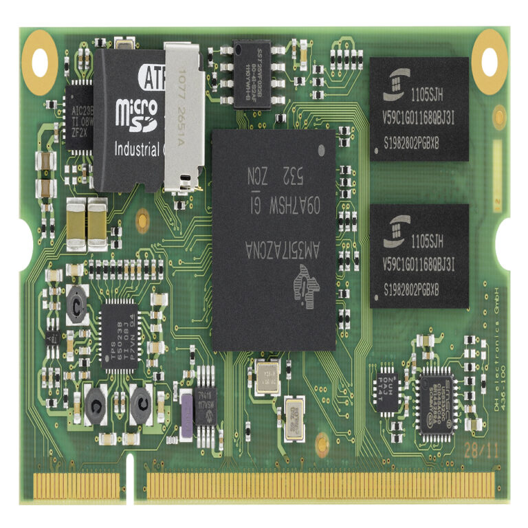
HDI PCB board, refers to High Density Interconnect, that is, high density interconnect boards. HDI technology adapts and advances the development of the PCB industry, and has been widely used in many fields. As a leading manufacturer of high-reliability multilayer boards, SenvePCBA adheres to the core concept of ‘increasing efficiency and lowering costs for the electronics industry’, and creates high-end HDI boards of up to 20 layers and 1-3 steps with high-precision technology by using 0.1mm laser drilling and mature blind-embedded hole technology.
Craftsmanship is everlasting, and brand power is everlasting. We are the promoter and practitioner of the electronics industry. In the international context of the chip technology is limited for a long time, HDI technology has a profound significance for the innovation and development of the electronics industry.
Tabla de contenido
Perforación láser de 0,1 mm, rompiendo el límite de la tecnología tradicional.
HDI PCB boards are a new technology developed by the PCB industry at the end of the 20th century. The drilling of traditional PCB boards is affected by drilling knives, and when the drilling hole diameter reaches 0.15mm, it is already close to the limit. And HDI board drilling no longer rely on traditional mechanical drilling, Huaqiu circuit using 0.1mm laser drilling technology, pad size is greatly reduced, the unit area to get more line distribution, to achieve the true meaning of high-density interconnection.
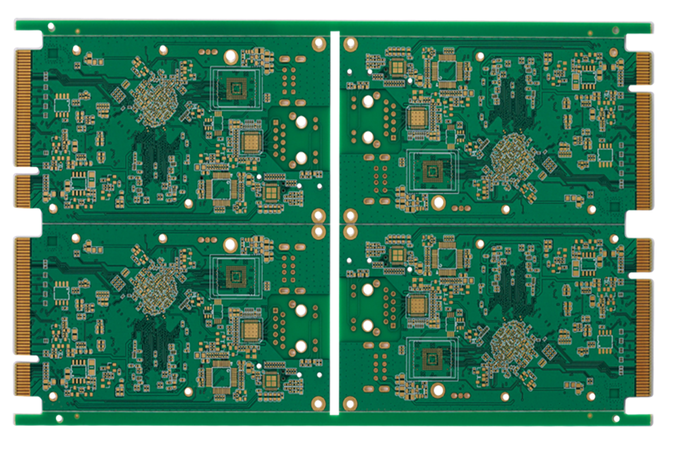
1-3 order HDI, mature blind buried hole technology, fully meet the design requirements.
Along with the continuous development of science and technology, as well as the continuous improvement of people’s demand for end-products, it is difficult to meet all the design needs of 1-stage HDI boards, and 2-stage and even higher-stage HDI has gradually become the core direction of the mainstream market. sevepcba has been focusing on the PCB industry for 13 years, and has made every effort to create high-reliability PCBs. through the mature blind-embedded vias with laser drilling and other high-precision processes, it can Sevepcba has been focusing on the PCB industry for 13 years, and is committed to building highly reliable PCBs.
What’s the Difference between HDI PCB and ordinary pcb ?
The core difference between HDI boards and ordinary PCBs lies in the manufacturing process, wiring density and electrical performance: HDI boards use laser drilling and micro-blind submerged hole technology to achieve higher density interconnections, which is suitable for scenes with stringent requirements for miniaturisation and high performance, whereas ordinary PCBs use the traditional mechanical drilling process, which is suitable for conventional electronic products.
Diferencias en el proceso de fabricación
- Drilling Technology:
HDI Board: Using laser drilling technology, the hole diameter can be as small as 0.076mm (3mil), breaking through the physical limitations of traditional mechanical drilling.
Ordinary PCB: relies on mechanical drilling, the smallest hole size is usually 0.15mm, and the cost increases significantly with the reduction of hole size.
- Hole Types:
HDI boards: use micro-blind, buried and stacked hole structures to save wiring space and reduce signal loss.
Ordinary PCB: Mainly use through holes throughout the board, taking up more wiring area.
Comparación de Estructura y Rendimiento
- Cabling Density
HDI board: line width/spacing up to 0.076mm/0.076mm (3mil/3mil), pad density over 130 points/square inch, supports dense packages such as BGA.
Ordinary PCB: line width/spacing is usually ≥ 0.1mm, wiring density is only 1/3~1/2 of HDI board.
- Rendimiento eléctrico
HDI boards: impedance control accuracy ±5%, 40% reduction in signal transmission loss, significant improvement in RF interference and thermal conduction.
Ordinary PCB: Weak signal integrity, suitable for low-frequency, low-complexity circuits.
Diferencias de aplicación y costo
- Aplicaciones típicas:
HDI boards: High-end products such as smartphones, 5G communication modules, medical imaging equipment, etc., which need to achieve high-speed signal transmission in limited space.
Ordinary PCB: basic electronic products such as home appliance control boards and LED lighting.
- Production cost:
HDI boards: using electroplating to fill holes, mSAP process, etc., the manufacturing cost is 30%-50% higher than that of ordinary PCBs.
Ordinary PCB: mature process, suitable for large-scale low-cost production
¿Cómo distinguir entre placas HDI PCB 1+N+1, 2+N+2 y 3+N+3?
The 1st, 2nd and 3rd order of HDI boards are mainly distinguished by the number of press-fit, laser drilling and process complexity, where the higher order represents higher manufacturing technology requirements and stronger inter-layer interconnection capability.
1+N+1 HDI PCB board
Manufacturing process: Single press lamination with single laser drilling. Blind holes connect neighbouring layers (e.g. 1-2 layers or outer and first inner layer). Structural characteristics: Small number of layers (usually 4-6). Shallow depth of blind holes, only partial interconnections. Application areas: General consumer electronics (e.g. Bluetooth headsets, smartwatch motherboards).
2+N+2 HDI PCB board
Manufacturing process: Twice pressed and twice laser drilled. Staggered or stacked holes (e.g. adjacent blind holes stacked to form cross-layer connections). Structural features: The number of layers is increased to around 8. Cross-layer interconnections of 1-3-5 layers are possible. Alignment accuracy and copper plating uniformity challenges need to be solved. Typical applications: Smart phones, tablet PCs, and other mid- to high-end devices.
3+N+3 HDI PCB board
Manufacturing process: Three or more presses and laser drilling. May include plating to fill holes, arbitrary layer interconnection technology. Technical Challenges: Control of interlayer offset due to multiple laminations. Precision requirements for drilling micro vias (<75μm). Risk of copper plating voids due to blind hole stacking. Application scenarios: 5G base stations, aerospace equipment, high-performance computing servers and other ultra-high-frequency fields.
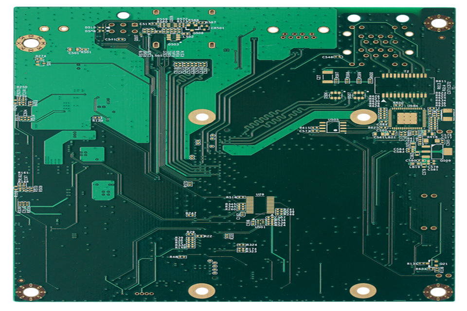
why HDI PCB board important for high-reliability applications?
HMicrovia and blind vias on HDI PCBs allow precise control of signal paths, shortening electrical connection distances and reducing signal degradation and interference caused by long distance transmission.
What are the key challenges in manufacturing high-reliability HDI PCBs?
High precision of microvia ,processing High difficulty of fine-pitch soldering ,Difficulty of precision control of multi-layer lamination ,Complicated signal integrity safeguard ,Tough thermal management design requirements
¿Cómo se asegura una fábrica confiable de PCB HDI del control de calidad?
AOI, X-ray inspection,high-Tg laminates), and conduct thermal cycling and stress tests.
¿Qué industrias se benefician más de las PCB HDI de alta fiabilidad?
telecommunications (5G infrastructure), automotive (ADAS, EVs), medical devices (imaging systems), and aerospace (satellite electronics)
¿Cómo se pueden prevenir los defectos de PCB HDI como cortocircuitos o deslaminación?
Defect prevention involves precise design rules (e.g., avoiding dense via clusters), advanced plating techniques for via reliability, and thorough cleaning processes to remove contaminants. Thermal management during lamination also reduces delamination
¿Qué debo buscar en un fabricante de PCB HDI de alta fiabilidad?
in HDI technologies, ISO certifications, access to cutting-edge equipment (e.g., laser drillers, 3D profiling tools)
Resumen
The production process of HDI pcb board differs greatly from that of traditional PCBs, and the higher the order of HDI technology, the more difficult it is, so we won’t talk about them one by one here. When a quality product can perfectly match the user’s needs, the product’s own value can be maximised. Sevenpcba has always adhered to the basic principle of ‘pursuing excellent quality and creating the ultimate user experience’, and we believe that high reliability HDI boards can satisfy the needs of more users.