Der Grundstein der intelligenten Fertigung: Panoramaanalyse der Leiterplattenmontagetechnologie im Jahr 2025 und Branchenausblick
Abstrakt
Dieser Artikel analysiert eingehend den Kernwert und den Entwicklungskontext der PCB-Montagetechnologie im Jahr 2025 sowie die Branchenaussichten (Leiterplattenbaugruppe)-Technologie und erläutert systematisch die Schlüsselelemente von den grundlegenden Prozessen bis hin zur industriellen Transformation. Der Schwerpunkt liegt auf der technologischen Entwicklung, die durch intelligente Fertigung und grüne Transformation vorangetrieben wird, kombiniert mit den Anforderungen von Spitzenbereichen wie 5G-Kommunikation, KI-Rechenleistung und intelligent vernetzten Fahrzeugen. Es analysiert die Durchbruchspfade innovativer Technologien wie High-Density Interconnection (HDI), flexibler Elektronik (FPC) und 3D-Verpackung.
Inhaltsverzeichnis
1. PCB-Montagetechnologiesystem: Der Evolutionspfad von Basisprozessen zur intelligenten Fertigung
1.1 Neuronales Netzwerksystem der Elektronikindustrie: Leiterplattenbestückungstechnologie
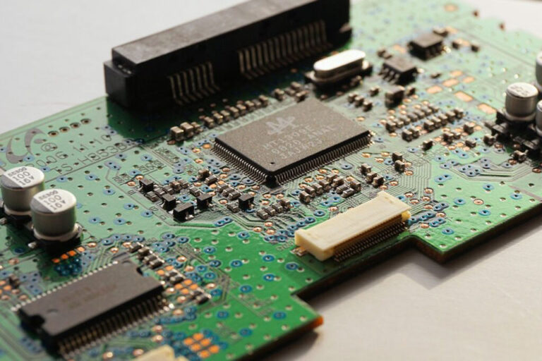
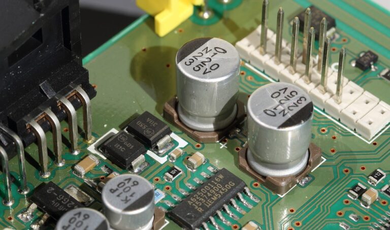
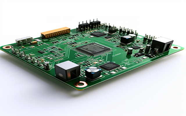
Als zentrales Nervensystem elektronischer Produkte trägt die Leiterplattenbestückung (PCBA) die Hauptaufgabe, die Schaltungsverbindung, Signalübertragung und Funktionsintegration zu realisieren. Der aktuelle Mainstream-Prozess stellt eine zweigleisig parallel Muster:
• Oberflächenmontagetechnik (SMT): Die Industriesäule, die 78% des Marktanteils einnimmt, unterstützt die Montage von 0402 (0,4 × 0,2 mm) Ultramikrokomponenten und die tägliche Einzellinienproduktion kann 5 Millionen Punkte erreichen
• Durchstecktechnik (THT): Hält einen 15%-Anteil in den Bereichen Automobilelektronik und industrielle Steuerung und unterstützt Hochstromübertragung und Szenarien mit hoher mechanischer Belastung
1.2 Dreifache Durchbrüche in der technologischen Revolution der PCB-Montagetechnologie
Im Jahr 2025 präsentiert die Branche Präzision, Flexibilität und Intelligenz drei wichtige Upgrade-Richtungen:
- Micro-Pitch-Verfahren: Linienbreite/Linienabstand durchbricht die 20-μm-Grenze und unterstützt die Verpackung von 5G-Millimeterwellen-Antennenarrays
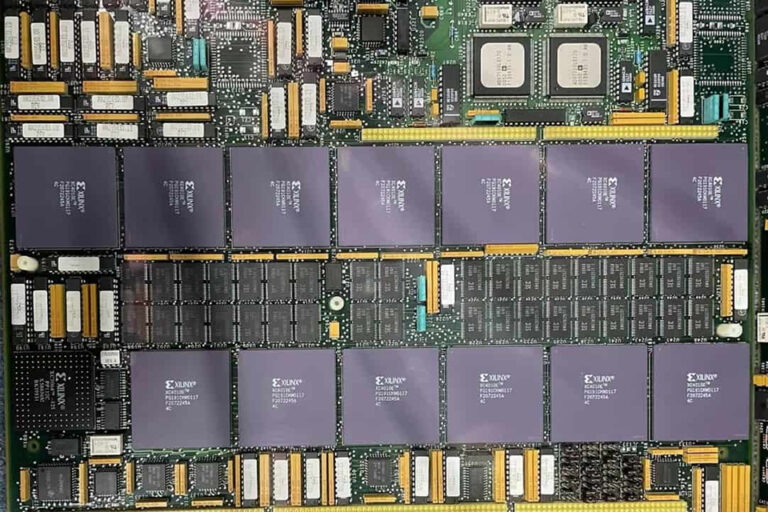
- Heterogene Integrationstechnologie: Der 3D-MID-Prozess realisiert die Integration einer elektromagnetischen Abschirmung und einer Wärmeableitungsstruktur, und die Komponentendichte wird um 40% erhöht
- Digitales Zwillingssystem: KI-Qualitätsprüfgeräte erreichen eine Fehlererkennung auf 0,01 mm-Ebene und erhöhen die Ausbeute auf 99,95%
2. Industrielle Ökologische Karte: Wettbewerbsfähige Durchbruchstrategien im Billionenmarkt
2.1 Rekonstruktion der regionalen Kapazitätsmatrix
China hat eine „Ein Kern und drei Pole“ Industrieanlage:
| Region | Kernvorteile | Repräsentative Unternehmen | Marktanteil
| |——-|—————-|—————-|———-| | Perlflussdelta | Ökologische Kette für Unterhaltungselektronik | Pengding Holdings, Shenzhen South Circuit | 42% | | Jangtse-Delta | Hochwertige Verpackungssubstrate | Shanghai Electric Co., Ltd., Shengyi Electronics | 35% | | Bohai Rim | Spezialplatinen für Militär, Luft- und Raumfahrt | Aerospace Circuit, Tianjin Prin | 18% |
2.2 Bewertungsmodell für die Lieferantenfähigkeit der Leiterplattenbestückungstechnologie
Die Auswahl eines PCBA-Dienstleisters erfordert den Aufbau eines Bewertungssystem „4C“:
• Technische Tiefe (Fähigkeit): Ob es die Fähigkeit hat, HDI-Blind- und Buried-Vias in beliebiger Reihenfolge sowie mehrschichtige Platinen mit über 100 Lagen in Massenproduktion herzustellen
• Intelligente Fertigungsebene (Konnektivität): Digitale Kennzahlen wie MES-Systemabdeckung und Gerätevernetzungsrate
• Qualitätskontrolle (Kontrolle): IATF 16949-Zertifizierung, CTQ-Schlüsselmerkmal-Kontrollprozess
• Ökologische Zusammenarbeit (Kooperation): Tiefe der strategischen Zusammenarbeit mit Material-/Ausrüstungslieferanten
3. Zukünftiges Schlachtfeld: Technische Durchbrüche in sieben aufstrebenden Wachstumspolen
3.1 KI-Rechenleistungsinfrastruktur
• Server-Motherboard: Der Wert einer einzelnen Leiterplatte für ein KI-Trainingsgehäuse übersteigt 12.000 Yuan, was die Nachfrage nach 112-Gbit/s-Hochgeschwindigkeits-Backplanes antreibt
• Verpackung optischer Module: Die Wärmemanagementlösung auf Kupfersubstrat für 800G OSFP-Komponenten erhöht die Wärmeableitungseffizienz um 60%
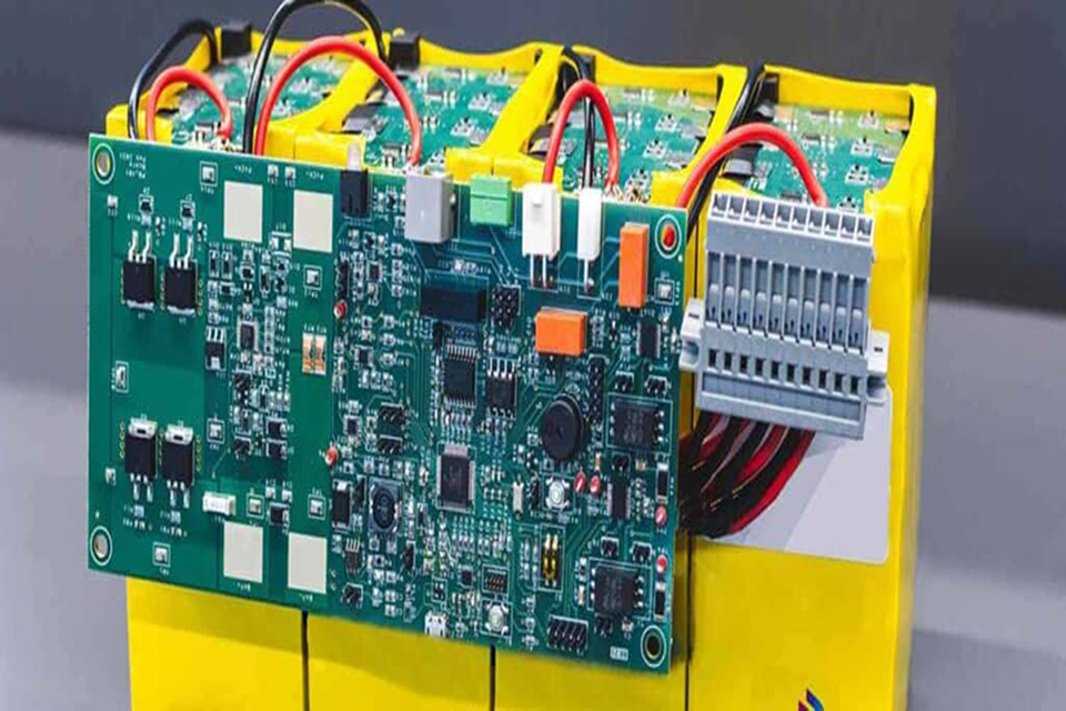
3.2 Leiterplattenmontagetechnologie für intelligent vernetzte Automobilelektronik
• Domänencontroller: 12 Schichten HDI beliebiger Ordnung werden zur Integration von ADAS- und Smart-Cockpit-Funktionen verwendet
• Batteriemanagementsystem: Das Kupfersubstrat hat eine Strombelastbarkeit von 300 A und einen Temperaturbereich von -40 °C bis 150 °C
3.3 Satelliteninternet-Netzwerke
• Phasengesteuerte Array-Antennenplatine: Dielektrischer Verlust des Ka-Band-Hochfrequenzsubstrats ≤0,002, erfüllt die Anforderungen für den Serieneinsatz von Satelliten in niedrigen Umlaufbahnen
• Strahlenresistente Verpackung: Es wird ein Polyimidsubstrat mit einer Gesamtdosistoleranz von 100 krad verwendet
4. Die große Mauer der Qualität: Aufbau eines Null-Fehler-Fertigungssystems
4.1 Digitaler Wandel der Prozessüberwachung
• Bildverarbeitungssystem: AOI-Geräte sind mit einer optischen Linse auf 10-μm-Ebene ausgestattet und verfügen über eine Fehlererkennungsrate von 99,8%
• Quantenpunktverfolgung: Implantierbare Nanomarker ermöglichen die vollständige Rückverfolgbarkeit von Materialien in der Leiterplattenmontagetechnologie
4.2 Zuverlässigkeitsüberprüfungsmatrix der PCB-Montagetechnologie
| Testkategorie | Kernindikatoren | Industriestandards |
|---|---|---|
| Thermische Belastung | 3000 Zyklen von -55 °C bis 125 °C | IPC-9701 |
| Mechanische Vibrationen | 20G Beschleunigung, 10–2000 Hz Wobbelfrequenz | MIL-STD-883 |
| Chemische Korrosion | 96-Stunden-Salzsprühtest | ISO 9227 |
5. FAQ: Lösung der Kernprobleme der Branche
Can SMT completely replace THT technology?
A: Im Bereich der elektronischen Leistungsmodule für Kraftfahrzeuge (z. B. IGBT-Treiberplatinen) und Industriesteckverbinder bietet THT nach wie vor unersetzliche Vorteile hinsichtlich der mechanischen Festigkeit. Es wird empfohlen, Hybridverfahren um die beste Kosteneffizienz zu erreichen.
How to reduce the dielectric loss of high-frequency materials for PCB assembly technology ?
Rogers RO4835 material is modified by ceramic filling, and the Dk value is stable at 3.0±0.05, and the loss tangent is ≤0.0025, which is particularly suitable for 77GHz millimeter wave radar applications.
How to evaluate the supplier’s rapid response capability?
Focus on the NPI-Zyklus (Einführung neuer Produkte)Führende Unternehmen können eine 72-stündige Hochschichtplattenprüfung durchführen und verfügen über ein professionelles DFM-Analyseteam.
How to ensure the reliability of lead-free welding of PCB Assembly technology ?
Using SAC305 solder alloy + nitrogen reflow process, the tensile strength of the solder joint reaches 45MPa, which meets the AEC-Q004 automotive regulations.
What are the difficulties in flexible electronic assembly?
A: Der Schlüssel liegt in der CTE-Anpassung des PI-Substrats. Dazu sind ein kombinierter Prozess aus Laserbohren (<50 μm) und anisotropem leitfähigem Klebstoff (ACP) erforderlich.
How to deal with fluctuations in raw material prices?
A: Durch die Einrichtung eines vertikalen Integrationssystems aus Kupferfolie, kupferkaschiertem Laminat und Leiterplatten, wie etwa dem Modell der Jiantao Group, können die Gesamtkosten um 12% gesenkt werden.
6. Technology Outlook: 2030 Development Roadmap
- Quantenverbindungstechnologie: Graphensubstrat ermöglicht Signalübertragung auf THz-Niveau und reduziert Verluste um 90%
- Biologisch abbaubares Substrat: Zellulose-Nanofaserplatten haben einen natürlichen Abbauzyklus von ≤6 Monaten
- Selbstreparierendes Schaltungssystem: Die Mikrokapselstruktur ermöglicht die automatische Reparatur von Stromkreisunterbrechungen und verlängert die Lebensdauer um das Fünffache
Zusammenfassung
Die Leiterplattenbestückungstechnologie erlebt einen qualitativen Sprung von Fertigungswerkzeug Zu InnovationsmotorAngesichts neuer Herausforderungen wie der KI-Rechenleistungsinfrastruktur, der 6G-Kommunikation und der Gehirn-Computer-Schnittstelle müssen Unternehmen Technologie-Qualität-Ökologie dreidimensionale Wettbewerbsfähigkeit. Es wird empfohlen, sich auf drei strategische Richtungen zu konzentrieren:
① Inländischer Ersatz von Hochfrequenz- und Hochgeschwindigkeitsmaterialien
② Zertifizierung der funktionalen Sicherheit von Automobilelektronik
3. Forschung und Entwicklung spezieller Karten für Satelliteninternet. Nur wenn wir das Zeitfenster der technologischen Iteration nutzen, können wir in dieser elektronischen industriellen Revolution die Oberhand gewinnen.