-
Xinxintian Industrial Zone, Shajing Street,Bao'an District, Shenzhen, China

PCB Assembly for IoT and Wearable Devices: The Rise of Miniaturization
[ad_1]
PCB Assembly for IoT and Wearable Devices: The Rise of Miniaturization
The Internet of Things (IoT) and wearable devices have revolutionized the way we live and interact with technology. With the increasing demand for smaller, more efficient, and cost-effective devices, PCB assembly has become a crucial aspect of the manufacturing process. In this article, we will explore the rise of miniaturization in PCB assembly for IoT and wearable devices, and the challenges and opportunities that come with it.
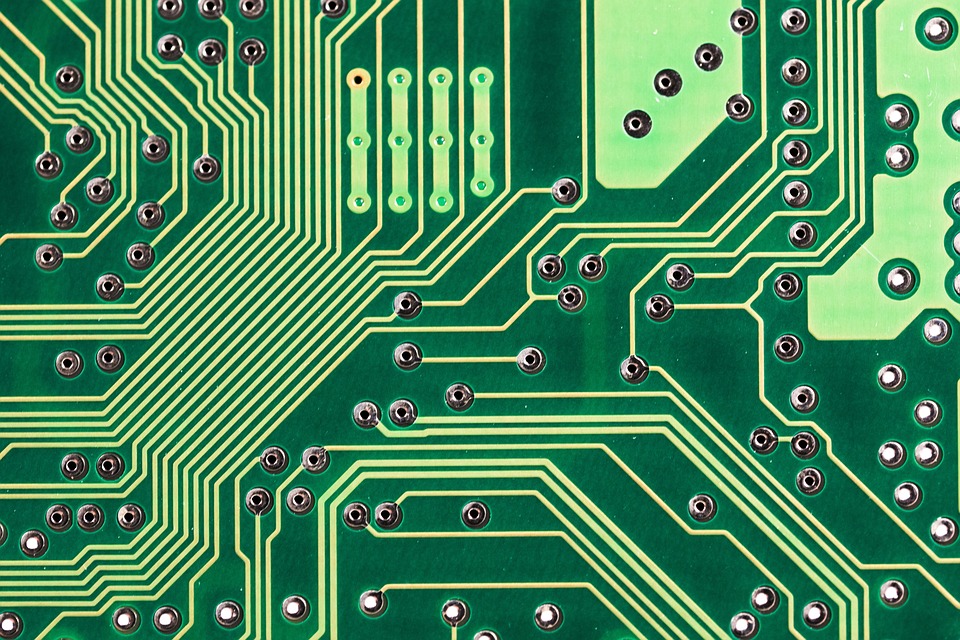
Miniaturization in PCB Assembly
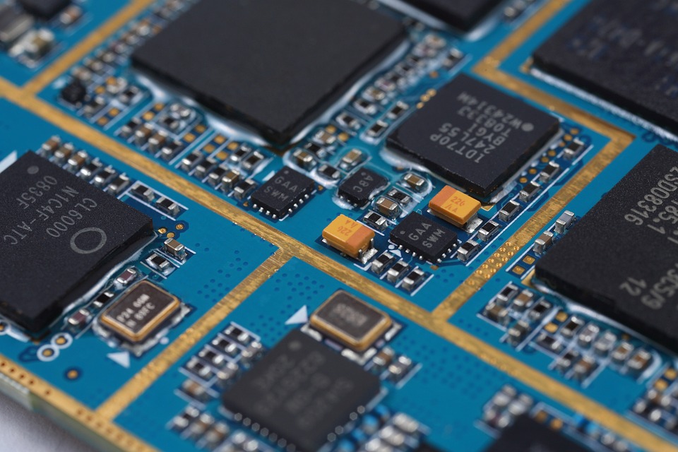
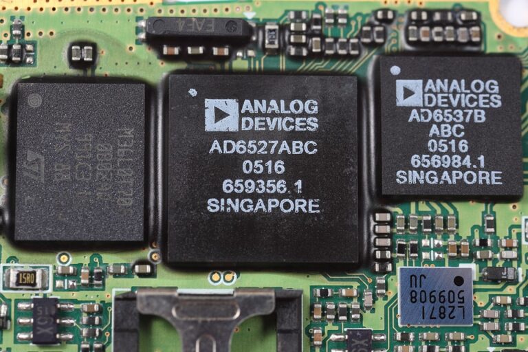
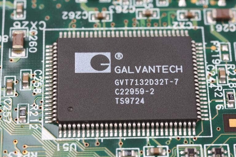
Miniaturization in PCB assembly refers to the process of reducing the size of printed circuit boards (PCBs) while maintaining their functionality. This trend has been driven by the increasing demand for smaller and more portable devices, such as smartwatches, fitness trackers, and wearable cameras. To achieve miniaturization, PCB manufacturers have developed new technologies and techniques, such as:
- Smaller components**: The development of smaller components, such as chip resistors and capacitors, has enabled the creation of smaller PCBs. These components are designed to operate at higher frequencies and with greater precision, making them ideal for use in miniaturized PCBs.
- Advanced manufacturing techniques**: Advanced manufacturing techniques, such as laser drilling and precision printing, have enabled the creation of smaller and more complex PCBs. These techniques allow for the precise placement of components and the creation of intricate designs.
- Conductive inks**: Conductive inks have been developed to enable the creation of flexible and wearable devices. These inks are designed to be flexible and can be printed onto a variety of materials, including fabric and plastic.
Challenges of Miniaturization
While miniaturization has brought many benefits to PCB assembly, it also presents several challenges. Some of the key challenges include:
- Component selection**: The selection of components that are suitable for miniaturized PCBs is a significant challenge. Components must be designed to operate at higher frequencies and with greater precision, and must be compatible with the smaller PCB design.
- Thermal management**: Miniaturized PCBs can generate significant heat, which can be challenging to manage. Thermal management is critical to ensure that the device operates within its specified temperature range.
- Reliability and durability**: Miniaturized PCBs are more prone to failure due to their smaller size and increased complexity. Reliability and durability are critical to ensure that the device operates reliably over its lifespan.
Opportunities in PCB Assembly for IoT and Wearable Devices
Despite the challenges, miniaturization in PCB assembly presents several opportunities for the development of new and innovative devices. Some of the key opportunities include:
- Wearable devices**: The development of wearable devices, such as smartwatches and fitness trackers, has driven the demand for miniaturized PCBs. These devices require small, lightweight, and low-power PCBs that can operate for extended periods of time.
- IoT devices**: The development of IoT devices, such as smart home devices and industrial sensors, has also driven the demand for miniaturized PCBs. These devices require small, low-power, and low-cost PCBs that can operate reliably in a variety of environments.
- Healthcare and medical devices**: Miniaturized PCBs are being used in healthcare and medical devices, such as pacemakers and implantable sensors. These devices require small, reliable, and durable PCBs that can operate in the human body.
Conclusion
In conclusion, miniaturization in PCB assembly is a critical aspect of the manufacturing process for IoT and wearable devices. While it presents several challenges, it also presents several opportunities for the development of new and innovative devices. To overcome the challenges and capitalize on the opportunities, PCB manufacturers must continue to develop new technologies and techniques, and must work closely with designers and engineers to ensure that the devices meet the required specifications.
FAQs
- Q: What is miniaturization in PCB assembly? A: Miniaturization in PCB assembly refers to the process of reducing the size of printed circuit boards (PCBs) while maintaining their functionality.
- Q: What are the challenges of miniaturization in PCB assembly? A: The challenges of miniaturization in PCB assembly include component selection, thermal management, and reliability and durability.
- Q: What are the opportunities in PCB assembly for IoT and wearable devices? A: The opportunities in PCB assembly for IoT and wearable devices include the development of wearable devices, IoT devices, and healthcare and medical devices.
- Q: How can PCB manufacturers overcome the challenges of miniaturization? A: PCB manufacturers can overcome the challenges of miniaturization by developing new technologies and techniques, and by working closely with designers and engineers to ensure that the devices meet the required specifications.
[ad_2]

admin
You may also like

PCB Design for Manufacturing (DFM): Streamlining the Design-to-Manufacturing Process
High-Speed PCB Design: Techniques and Considerations for Fast and Reliable PCBs – Strategies for designing PCBs that can handle increased signal speeds and data transfer rates.
PCB Design Software: A Comparison of Popular Tools and Features