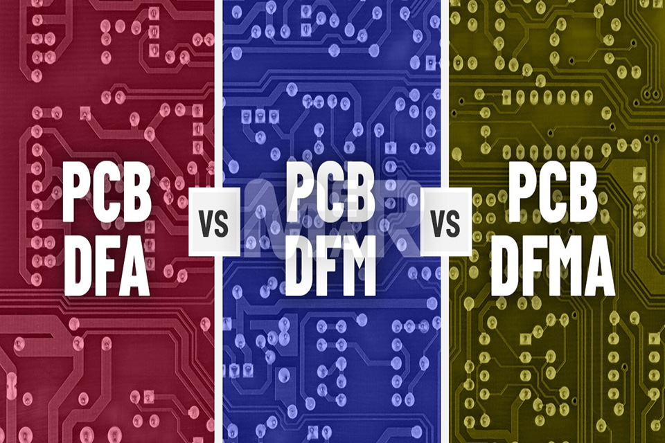
ما هي أدوار ووظائف DFT و DFM و DFA في PCB؟
مقدمة
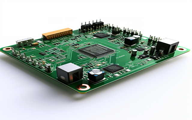
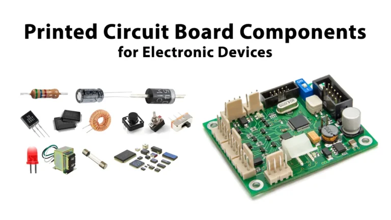
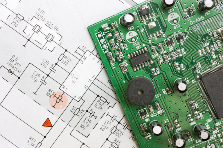
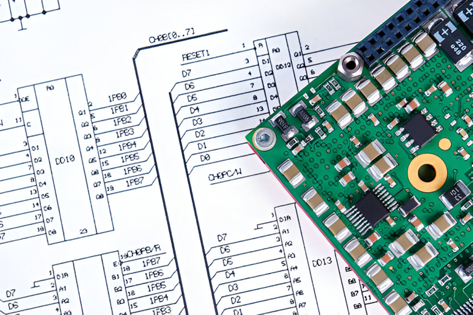
In the field of modern electronic manufacturing, the high quality and efficiency of PCB service (printed circuit board service) depends on three core design principles: DFT (design for testability), سوق دبي المالي (design for manufacturability), and DFA (design for assembly). These design methods run through the entire life cycle of لوحة الدوائر المطبوعة (printed circuit board) from concept to mass production, directly affecting the reliability, production cost, and market competitiveness of the product. This article will deeply analyze the core functions of these three technologies, explore how they can jointly optimize the تصميم لوحة الدوائر المطبوعة process, and help engineers and manufacturers make more informed decisions through actual cases and data comparisons.
جدول المحتويات
The core value of DFT, DFM, and DFA
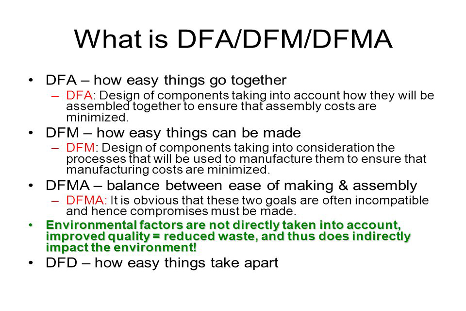
DFT, DFM, and DFA are the three pillars in the field of electronic design, targeting the optimization needs of testing, manufacturing, and assembly respectively. Their common goals are: Reducing failure rates, shortening development cycles, and controlling costs.
DFT (Design for Testability) – Ensure product reliability
DFT By embedding test logic in the design stage, it ensures that PCB can quickly and accurately detect manufacturing defects and functional failures.
Key functions of DFT
- Fault detection and diagnosis
- Functional defects: Such as short circuits, open circuits or component parameter deviations, can be located by capturing current, voltage and temperature data through test points.
- Failure mode analysis: Identify repetitive errors (such as signal interference or power supply fluctuations) and optimize circuit design.
- Manufacturing defect prevention
- Temporary test technology: No need to modify the original design, verify circuit performance through temporary test points, and reduce later rework.
- ICT test: Use a bed of nails fixture to detect parameters such as resistance and capacitance, which is suitable for mass production.
- FCT test: Functional verification test, simulating circuit performance in a real working environment.
- X-ray test
- Used to detect defects in hidden solder joints such as BGA (ball grid array) to ensure welding quality.
DFT test technology comparison table
| Test type | السيناريوهات القابلة للتطبيق | Detection accuracy | فعالية التكلفة |
|---|---|---|---|
| تكنولوجيا المعلومات والاتصالات | Mass production | عالي | عالي |
| مقاطعة العاصمة الفيدرالية | Functional verification | واسطة | واسطة |
| الأشعة السينية | Hidden solder joint detection | Very high | قليل |
DFM (Design for Manufacturability) – Optimize manufacturing process
سوق دبي المالي aims to ensure that PCB design is compatible with manufacturing processes, reduce production complexity and reduce risks.
Core principles of DFM
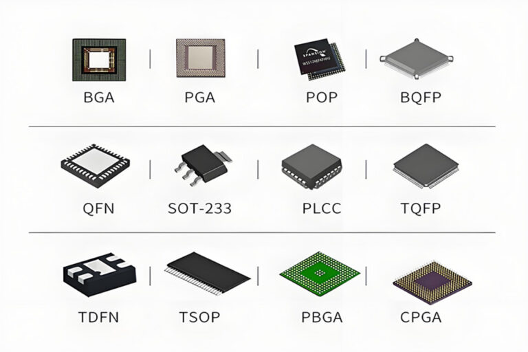
- Component selection and layout
- Give priority to the use of standardized components and reduce unique package types (such as BGA vs. QFP).
- Reasonably plan the trace width (≥6mil), via spacing (≥8mil) and power layer segmentation to avoid electromagnetic interference (EMI).
- استراتيجية ضبط التكاليف
- Reduce the number of layers: Double-sided boards are 30%-50% cheaper than multi-layer boards, but signal integrity requirements need to be weighed.
- Multi-purpose design: For example, the ground layer serves as both EMI shielding and structural support.
- EMC design specifications
- Plan electromagnetic compatibility (EMC) parameters in advance to avoid rework due to signal crosstalk later.
DFM design points
| Design elements | Recommended values | وظيفة |
|---|---|---|
| Minimum trace width | ≥6mil | Prevent short circuit |
| Via spacing | ≥8mil | Avoid poor welding |
| Board edge clearance | ≥5mm | Facilitate assembly and transportation |
###H2: DFA (Design for Assembly) – Improve assembly efficiency DFA Reduce the error rate of manual assembly by simplifying component layout and standardizing processes.
DFA implementation method
- Standardized design
- Reduce component types: For example, use 0805 package resistors uniformly to avoid mixing multiple sizes.
- Verify component sources: give priority to certified suppliers to avoid the risk of counterfeit parts.
- Eliminate assembly errors
- Tolerance control: Drilling size error must be ≤±5μm, in line with IPC-6012 standards.
- Heat release design: Add heat dissipation holes in high-temperature areas to prevent welding deformation.
DFA advantage comparison
| Traditional design | DFA optimized design | Improved effect |
|---|---|---|
| Manual welding of 100 components | Automatic welding of 80 components | Save 20% time |
| 3 types of packages | 1 standardized package | Reduce 40% error rate |
Synergy of DFT, DFM, and DFA
These three technologies do not exist in isolation, but are interrelated:
- DFT relies on DFM: The layout of test points must meet manufacturing process constraints.
- DFM supports DFA: Standardized design simplifies the assembly process.
- DFA Feedback DFT: Assembly error data can be used to optimize test strategies.
Frequently Asked Questions (FAQ)
Will DFT increase PCB costs?
In the short term, the test points will increase a small amount of cost, but in the long term, rework losses can be reduced and the overall cost will be reduced.
How does DFM affect the selection of PCB layers?
High-frequency signals or high-density wiring may require more than 4 layers, but cost and performance need to be balanced.
Does the standardization of DFA limit design flexibility?
Standardized component libraries can speed up design, but 10%-15% of customization space needs to be reserved to accommodate special needs.
What PCB types are suitable for X-ray testing?
Mainly used for hidden solder joint detection such as BGA and CSP, not suitable for single-sided boards.
How does DFM optimize EMI issues?
Through power layer segmentation, signal line shielding and impedance matching design.
What is the difference between DFT and FCT?
ICT detects hardware parameters, FCT verifies functional performance, and the combination of the two can cover more than 95% of defects.
ملخص
DFT, DFM, and DFA are indispensable design principles in PCB services. They improve product reliability and efficiency from the perspectives of testing, manufacturing, and assembly. Through the analysis of this article, readers should grasp the following core points:
- DFT Detect manufacturing defects in advance by embedding test logic.
- سوق دبي المالي Optimize layout and material selection to reduce production costs.
- DFA Standardize components and processes to reduce assembly errors.
- The three can work together to shorten the development cycle by 30%-50% and increase the yield rate by 15%-25%.